
Quick Answer: You can prevent ceramic PCB warping by strictly balancing the top and bottom copper layers to a volume ratio of 0.9–1.1 and applying slow, controlled cooling profiles from the 1065°C bonding temperature. Unbalanced boards with a volume ratio above 1.3 will exponentially bow, exceeding the 0.1mm per 25mm flatness limit required for safe die-attach assembly.
Key takeaways:
- Thermal mismatch between alumina (6.9 ppm/°C) and copper (16.4 ppm/°C) triggers warping during cool-down.
- Bottom dummy copper planes resolve 90% of asymmetry-driven bowing issues.
- A ceramic-to-copper thickness ratio ≥2.0 significantly minimizes physical distortion.
- Laser profilometry guarantees 100% flatness compliance before assembly begins.
Table of Contents
- What Are the True Causes of Ceramic PCB Warping?
- Why Does Copper Volume Ratio Dictate Substrate Flatness?
- How Do You Calculate and Balance Copper Symmetries?
- What Are the Acceptable Flatness Specs for Die-Attach?
- How Do Design Changes Prevent Ceramic PCB Warping?
- Which Measurement Methods Accurately Detect Bow and Twist?
- How Does Controlled Cooling Relieve Post-Bonding Stress?
- What Happens to Assembly Yield When Boards Arrive Warped?
- How Do You Create a Flatness Specification Template?
- Can You Fix Ceramic PCB Warping After Fabrication?
You can eliminate ceramic PCB warping by balancing the top and bottom copper volume ratio to exactly 0.9–1.1 and applying controlled cooling profiles during the eutectic bonding phase. Many hardware engineers face massive yield losses when thick copper planes peel or bow substrates right off the assembly line. The root cause usually traces back to ignored ceramic PCB manufacturer layout rules regarding symmetry. This technical guide outlines the physics behind thermomechanical stress and provides exact design countermeasures to keep your power modules perfectly flat.
What Are the True Causes of Ceramic PCB Warping?
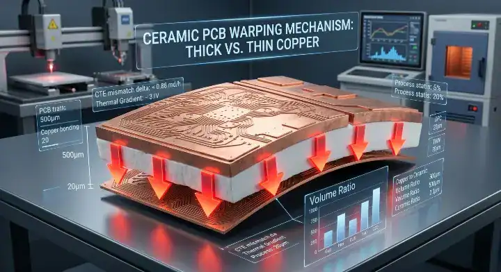
Ceramic PCB warping primarily occurs because copper contracts at a rapid rate of 16.4 ppm/°C, while alumina ceramic contracts at just 6.9 ppm/°C during the cool-down from 1065°C bonding temperatures. This CTE mismatch forces the substrate to permanently bow toward the side containing thicker or denser copper.
Why Does Stress Lock In During Cool-Down?
Hardware forums frequently host this exact user frustration: “Since there is a serious CTE mismatch between ceramic (Al₂O₃: 6.9 ppm/°C) and copper (16.4 ppm/°C), undesirable cracking and warpage may result” (Source: IEEE/EEVBlog). The physics dictate that warping is locked in during the cool-down phase from the bonding temperature, not during actual field use. At 1065°C for DBC (Direct Bonded Copper) or 800°C for AMB, both materials are fluid and stress-free.
Here is the reality: The residual stress becomes permanent the moment the metals solidify.
- Copper shrinks aggressively.
- The rigid ceramic resists the pull.
- The entire assembly bends to relieve the tension.
- Thicker copper inherently causes more severe warping.
How Does Copper Thickness Amplify the Bow?
When one side of the substrate houses a massive 300µm copper power plane and the other side holds only a thin signal layer, the tension becomes completely one-sided. AMB vs DBC base materials react differently, but the asymmetric pulling force always dictates the direction of the bow. The board will concave toward the heavier copper mass.
Key Takeaway: You must acknowledge that post-bonding stress is permanent and cannot be reversed. Bottom line: Always treat copper layout symmetry as a structural requirement, not just an electrical one, to prevent physical substrate distortion.
| Material | Coefficient of Thermal Expansion (CTE) | Bonding Temperature |
|---|---|---|
| Copper | 16.4 ppm/°C | N/A |
| Alumina (Al₂O₃) | 6.9 ppm/°C | 1065°C (DBC) |
| Silicon Nitride (Si₃N₄) | 2.6-3.2 ppm/°C | 800°C (AMB) |
If you use Si₃N₄, the CTE gap is even larger than Al₂O₃, meaning you must enforce even stricter symmetry rules to prevent bowing.
Why Does Copper Volume Ratio Dictate Substrate Flatness?
Maintaining a strict ceramic PCB warping copper volume ratio between 0.9 and 1.1 suppresses warpage by equalizing the thermal contraction forces on both sides of the dielectric layer. Ratios exceeding 1.3 cause an exponential increase in substrate bow, virtually guaranteeing rejected parts on the assembly line.
How Do You Calculate the Metal Ratio?
Engineers often quote this patent data: “Controlling volume ratio of upper/lower metal layers within 0.9-1.1 suppresses warpage” (Source: Patent/AMOGREENTECH/Stack Exchange). The volume ratio is calculated precisely as: (top copper area × thickness) divided by (bottom copper area × thickness). When this mathematical ratio deviates from 1.0, mechanical tension forces the board to bend.
Do not ignore this: Even if your electrical schematic only requires top-side routing, you must design a bottom layer.
- Calculate total square millimeters of top copper.
- Calculate total square millimeters of bottom copper.
- Ensure the quotient falls strictly between 0.9 and 1.1.
Can Grooves Fix the Imbalance?
When a full solid bottom plane makes the ratio too low, you can add non-functional grooves or etched slots to the bottom copper to fine-tune the remaining volume. This directly drops the physical mass pulling against the ceramic core.
Key Takeaway: The mathematical balance of top and bottom copper volume dictates the mechanical flatness of the board. Bottom line: Never approve a ceramic layout unless the calculated upper/lower metal volume ratio sits between 0.9 and 1.1.
| Copper Volume Ratio (Top:Bottom) | Expected Substrate Behavior | Assembly Suitability |
|---|---|---|
| 0.9 to 1.1 | Flat (<0.4% bow) | Ideal for all SMT / Die-attach |
| 1.1 to 1.3 | Slight bow (0.4% – 0.7%) | Risky for large bare dies |
| > 1.3 | Severe warping (>1.0% bow) | High probability of reject |
Because ratios over 1.3 generate extreme tension, you must redesign the layout before releasing the Gerber files to fabrication.
How Do You Calculate and Balance Copper Symmetries?
You balance ceramic PCB warping forces by matching the copper area coverage on the bottom layer to the top layer, aiming for a 1:1 volume ratio. According to IEEE research, a ceramic-to-copper thickness ratio ≥2.0 yields significantly less warpage than a ratio <1.5.
What Happens When Designs Are Asymmetrical?
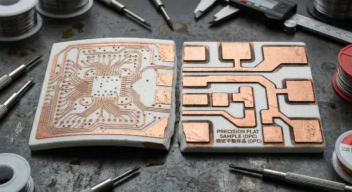
When you evaluate a ceramic PCB manufacturer, ask how they handle asymmetric designs. A SiC power module designer came to us with severe warping on a 40mm × 50mm DBC Al₂O₃ board. The top side featured 300µm copper at 85% coverage, while the bottom had only a 30% ground plane.
Consider the math: The copper volume ratio was a massive 2.8:1.
- This caused a 0.35mm bow.
- Solder paste printing became impossible.
- Production stalled immediately.
How We Fixed a SiC Module Layout?
We provided our free DFM/DFA engineering review and redesigned the bottom copper layer. We added non-functional fill zones with 0.3mm etched slots to bring the bottom coverage up to 80%, achieving a highly stable 1.06:1 volume ratio.
Key Takeaway: Intelligent addition of dummy copper directly counteracts thermal tension without altering electrical performance. Bottom line: Use slotted dummy copper planes on the bottom side to artificially balance heavy top-side power routing.
| Design Stage | Copper Ratio (Top:Bottom) | Measured Bow | Die-Attach Yield |
|---|---|---|---|
| Original Design | 2.8 : 1 | 0.35mm | 72% |
| Optimized Design | 1.06 : 1 | 0.04mm | 97% |
By correcting the copper symmetry to 1.06:1, the design easily passed the ±0.08mm spec, increasing final yield to 97% with zero added unit cost.
What Are the Acceptable Flatness Specs for Die-Attach?
The industry standard for controlling ceramic PCB warping during high-precision die-attach applications is a maximum bow of less than 0.1mm per 25mm of board length, equaling a 0.4% flatness ratio. Standard SMT components tolerate up to 0.75%, but bare dies will crack under that bending stress.
Why Do Bare Dies Require Stricter Specs?
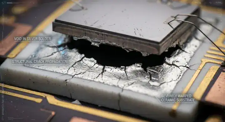
Bare silicon carbide (SiC) or gallium nitride (GaN) dies attach directly to the ceramic substrate without the buffer of a plastic IC package. If the substrate bows by more than 0.1mm, the extremely thin solder or silver sintering layer beneath the die becomes uneven.
The result is clear: Voids form instantly.
- Heat accumulates in the voided areas.
- The die overheats and fails prematurely.
- The entire power module requires scrapping.
How Do Specs Vary By Application?
LED modules and high-power RF boards also demand strict 0.4% flatness limits to ensure optical alignment and impedance stability. Conversely, simple sensor boards using standard packaged components can function perfectly well with up to 0.75% bow without compromising solder joints.
Key Takeaway: The specific assembly technology dictates how much substrate bending you can tolerate. Bottom line: Specify a strict 0.4% maximum bow tolerance on your manufacturing drawings whenever your assembly includes bare die-attach or high-density BGA components.
| Application Type | Acceptable Flatness Limit | Primary Risk if Exceeded |
|---|---|---|
| High-Power Bare Die | < 0.4% (0.1mm / 25mm) | Die cracking, thermal voids |
| RF / LED Modules | < 0.5% (0.12mm / 25mm) | Optical misalignment |
| Standard SMT Packages | < 0.75% (0.18mm / 25mm) | Open solder joints |
Because bare dies lack package compliance, applying a 0.4% flatness limit prevents thermal voids from destroying the semiconductor.
How Do Design Changes Prevent Ceramic PCB Warping?
Engineers prevent ceramic PCB warping during the layout phase by adding dummy copper planes to the bottom side of the board, directly countering the thermal pull of the top-side traces. This simple ceramic PCB design rules DFM adjustment adds minimal cost but drastically reduces manufacturing rejection rates.
Should You Add Dummy Copper?
Warping is the single most common quality complaint we see on incoming DBC boards, with roughly 18% of initial supplier substrates arriving with a bow exceeding 0.15mm/25mm. We solved this in our full turnkey service by requiring every supplier to ship substrates with a matched bottom copper plane.
Here is the exact strategy: We enforce this even for single-side-only electrical designs.
- We add a non-net copper pour to the bottom layer.
- We match the top layer’s copper weight exactly.
- We use a grid pattern to match the volume percentage.
What Are the Best Design Countermeasures?
The dummy bottom copper adds approximately $0.30 to $0.50 per substrate in material costs. However, this microscopic investment reduces the incoming mechanical reject rate from 18% down to under 2%, easily paying for itself by saving expensive downstream components.
Key Takeaway: Proactive layout adjustments eliminate the physical physics of thermal tension before fabrication begins. Bottom line: Always include a symmetrical, non-functional bottom copper plane in your CAD tool to mechanically stabilize high-power ceramic substrates.
| Countermeasure | Implementation Difficulty | Effectiveness | Added Cost per Unit |
|---|---|---|---|
| Add dummy bottom copper | Very Low | Extremely High | $0.30 – $0.50 |
| Grid/Slot heavy planes | Low | High | $0.00 |
| Increase ceramic thickness | Medium | Moderate | $1.00 – $3.00 |
Adding dummy copper remains the most cost-effective solution, driving defect rates down by 16% for mere pennies per board.
Which Measurement Methods Accurately Detect Bow and Twist?
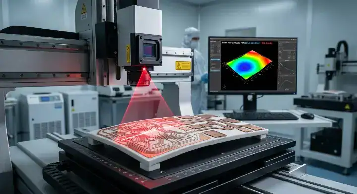
Laser profilometry is the most accurate method for measuring ceramic PCB warping, capturing continuous 3D surface topologies with sub-micron precision to detect subtle bows across the substrate. Coordinate Measuring Machines (CMM) are also effective but rely on slower, contact-based point measurements.
How Does Laser Profilometry Work?
A laser scans the entire surface area of the panel, generating a high-resolution topographical map. This technology immediately identifies whether the substrate exhibits a simple bow (bending on one axis) or a complex twist (warping across diagonal corners).
The advantage is speed: We run 100% incoming flatness scans using laser profilometers.
- It takes seconds per panel.
- It eliminates human measurement error.
- It catches microscopic deviations instantly.
Is CMM Still Relevant?
We once caught a 500-piece AlN-DBC lot with a 0.22mm bow resulting from a supplier’s cooling rate issue. The laser scan detected it before assembly began, avoiding approximately $15,000 in downstream SMT and die-attach scrap. While CMM is highly accurate, it is too slow for 100% volume screening.
Key Takeaway: Non-contact optical scanning provides the only viable path to guaranteeing flatness across large production volumes. Bottom line: Demand your factory utilizes laser profilometry for 100% outgoing inspection rather than relying on random batch sampling.
| Measurement Method | Speed | Accuracy Level | Best Use Case |
|---|---|---|---|
| Laser Profilometry | Very Fast | Sub-micron | 100% volume production |
| CMM (Contact) | Slow | Extremely high | NPI qualification |
| Go/No-Go Gauge | Instant | Low (Threshold only) | Rough incoming checks |
Because laser profilometry offers both extreme speed and sub-micron accuracy, it is the only method suitable for 100% inspection of high-reliability orders.
How Does Controlled Cooling Relieve Post-Bonding Stress?
Slowing the cool-down rate from 1065°C to room temperature reduces ceramic PCB warping by giving the copper layers more time to plastically yield, relieving residual thermomechanical stress. Rapid quenching locks in extreme tension, immediately causing the ceramic core to bow or suffer from ceramic PCB copper peeling.
What Is the Ideal Cooling Profile?
The eutectic bonding phase melts the metal to the ceramic, but the actual damage occurs during the return to ambient temperature. If a factory pushes panels through the cooling zone too quickly to speed up production, the rapid temperature drop violently contracts the copper.
The physics are unforgiving:
- The copper shrinks instantly.
- The ceramic matrix cannot flex.
- The stress exceeds the material’s yield point.
Does Annealing Help?
A highly controlled, stepped cooling profile allows the copper structure to anneal naturally as it cools. This gradual reduction in temperature dissipates the stored energy, resulting in a substrate that remains flat and structurally sound even under future thermal cycling.
Key Takeaway: Factory thermal management is just as critical as your layout geometry. Bottom line: Audit your supplier’s furnace profiles to ensure they utilize slow, stepped cooling zones rather than rapid quenching methods.
| Cooling Profile Type | Stress Relief | Final Warpage Risk | Production Speed |
|---|---|---|---|
| Slow / Stepped Cooling | Excellent | Very Low (<0.2%) | Slower |
| Standard Linear Cooling | Moderate | Medium (0.4%) | Average |
| Rapid Quenching | Poor | Extremely High (>1.0%) | Very Fast |
While rapid quenching increases factory output, it results in extremely high warpage rates that destroy assembly yields.
What Happens to Assembly Yield When Boards Arrive Warped?
Severe ceramic PCB warping prevents solder paste stencils from sealing flat against the board, causing paste bleeding, massive solder voiding, and ultimately dropping assembly yields below 70%. Warped boards also prevent high-power semiconductor components from making full thermal contact with bottom heat sinks.
How Does Bow Ruin Solder Printing?
In our PCB assembly operations, maintaining a 99.7% first-pass yield rate demands perfectly flat incoming materials. If a ceramic board has a 0.3mm bow, the metal stencil hovers above the center pads during the solder paste printing process.
This triggers a chain reaction:
- Solder paste bleeds under the stencil.
- Pads receive too much paste, causing bridges.
- Component placement pushes excess paste outward.
Will It Break During Pick-and-Place?
When the pick-and-place nozzle presses a heavy IGBT component down onto a bowed substrate, the mechanical force can instantly crack the rigid ceramic core. Furthermore, BGA components will suffer from open circuits because the corner balls hover above the downward-curving board surface. We run 3D AOI and X-Ray inspection on every BGA joint precisely to catch these height-related defects.
Key Takeaway: Substrate flatness directly dictates your final end-of-line manufacturing yield. Bottom line: Treat incoming substrate flatness as the most critical variable for guaranteeing high-yield solder paste printing and SMT placement.
| Defect Type | Root Cause on Warped Board | Yield Impact |
|---|---|---|
| Solder Bridging | Stencil gap causes paste bleed | High |
| Open BGA Joints | Board curves away from corner balls | Severe |
| Ceramic Cracking | Mounter nozzle crushes bowed center | Total Loss |
Because a warped board breaks the stencil seal, solder bridging becomes unavoidable, leading to massive rework costs.
How Do You Create a Flatness Specification Template?
You control ceramic PCB warping issues by explicitly defining a maximum bow of 0.4% and requiring a 100% laser flatness scan on your supplier Purchase Orders. Relying solely on IPC default standards is risky, because standard FR4 flatness tolerances are far too loose for precision ceramic die-attach.
What Data Goes Into the PO?
Never assume your supplier knows your internal assembly tolerances. Standard IPC-A-600 allows up to 0.75% bow and twist for surface mount boards, which is perfectly fine for basic FR4 but catastrophic for DBC substrates carrying bare SiC dies.
Specify these exact parameters:
- Maximum allowable bow: 0.4% (0.1mm per 25mm).
- Measurement method required: Laser Profilometry.
- Inspection volume: 100% of panels (no AQL sampling).
How Do You Enforce Incoming Quality?
Require the factory to provide the laser scan data report alongside the shipment. If the supplier refuses to guarantee a 0.4% flatness spec in writing, they likely lack the controlled cooling furnaces or the metrology equipment required to process high-end power electronics.
Key Takeaway: A rigid, written specification protects your budget from defective incoming materials. Bottom line: Explicitly override standard IPC tolerances on your fabrication drawings by mandating a maximum 0.4% bow and 100% outgoing flatness inspection.
| Specification Item | Standard IPC-A-600 | Required Ceramic Spec |
|---|---|---|
| Maximum Bow / Twist | 0.75% | ≤ 0.40% |
| Inspection Method | AQL Sampling | 100% Laser Scan |
| Reporting | Certificate of Compliance | Raw Scan Data Report |
By upgrading your PO requirements to 100% laser scanning, you shift the quality burden back to the manufacturer, saving your assembly line.
Can You Fix Ceramic PCB Warping After Fabrication?
No, you cannot fix ceramic PCB warping once the eutectic bonding process is complete, because the stress between the ceramic and copper is permanently locked into the material structure. Attempting to physically flatten a warped ceramic substrate in a hydraulic press will immediately shatter the brittle core.
Why Does Physical Pressing Fail?
Unlike standard FR4 materials, which have a glass transition temperature (Tg) allowing them to be baked and flattened under pressure, alumina and silicon nitride are crystalline structures. They possess zero elasticity at room temperature.
The reality is harsh:
- The copper holds the tension.
- The ceramic takes the load.
- Mechanical pressing fractures the ceramic matrix instantly.
Is Scrap the Only Option?
If a board arrives with severe warping that exceeds your stencil printing limits, the board must be scrapped. There is no thermal cycle or mechanical jig that can safely reverse a bad eutectic bond cool-down or fix a 3:1 copper volume imbalance after the fact.
Key Takeaway: Prevention during the layout and bonding phases is the only cure for substrate distortion. Bottom line: Stop attempting to salvage warped ceramic boards in assembly; redirect your engineering efforts toward fixing the copper volume ratio in the initial CAD layout.
| Rework Attempt | Immediate Result | Long-Term Reliability |
|---|---|---|
| Mechanical Pressing | Ceramic shatters | N/A (Destroyed) |
| Post-Baking | No change in shape | No improvement |
| Stencil Modification | Poor paste release | High risk of solder voids |
Because ceramic lacks elasticity, mechanical rework always fails, making upfront design symmetry your only defense.
Conclusion
Mastering the physics of thermomechanical tension ensures your high-power modules remain perfectly flat from the bonding furnace to final assembly. By strictly enforcing a 0.9–1.1 copper volume ratio, adding dummy copper to asymmetrical designs, and demanding 100% laser flatness scanning, you eliminate the delays and scrap costs associated with bent substrates.
At QueenEMS, we eliminate the guesswork from high-reliability manufacturing. We provide full turnkey EMS solutions—from rapid prototyping to mass production—utilizing up to 60-layer capabilities and advanced BGA X-Ray inspection to maintain a 99.7% first-pass yield. Stop fighting warped boards and start building reliable power modules. Contact us today for a free DFM review on your next thermal substrate project.
Written by the QueenEMS Engineering Team
Frequently Asked Questions
Can I fix a warped ceramic PCB by baking it in a reflow oven? No. Baking a ceramic substrate will not reverse warping. Because the CTE mismatch stress is permanently locked in during the 1065°C eutectic bonding phase, low-temperature reflow ovens (245°C) cannot generate enough heat to reset the metal’s mechanical structure.
What is the fastest way to balance my top and bottom copper layers? Calculate your total top copper area and mirror that exact square millimeter coverage on the bottom layer using a dummy copper plane. If the bottom plane becomes too heavy, add 0.3mm etched slots to reduce its mass until your volume ratio hits exactly 1.0.
How do I know if my ceramic PCB supplier has good cooling profiles? Request a sample batch of 10 boards and measure them with a laser profilometer. If the copper volume ratio is perfectly balanced at 1:1 but the boards still arrive with a bow exceeding 0.4%, the factory is utilizing rapid quenching rather than slow, controlled cooling.
Can I use standard FR4 flatness tolerances for my ceramic boards? No. Standard IPC-A-600 allows for up to 0.75% bow, which is acceptable for FR4 but will cause severe die-cracking and thermal voiding on bare SiC/GaN chips. You must explicitly specify a stricter 0.4% maximum bow on your fabrication drawings.
Does increasing the ceramic core thickness prevent bowing? Yes, but it reduces your thermal dissipation efficiency. While upgrading from a 0.38mm to a 0.63mm alumina core adds rigidity against the pulling force of the copper, it also drastically increases the thermal resistance of your power module. Balance the copper first before thickening the core.
Upload your files today · Free DFM check before production · Ship worldwide
Get your PCB prototypes in as fast as 24 hours. We handle FR4, Rogers, and Flex up to 60 layers — free prototypes for 2–4 layer boards, no minimum order.
Just upload your Gerber + BOM — we source every part, assemble, and inspect (AOI + X‑Ray) so you don't have to chase suppliers. Boards ship in as fast as 24 hours.