
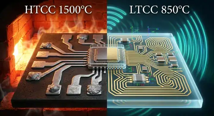
Quick Answer: The core difference between an HTCC vs LTCC ceramic PCB is the firing temperature and conductor material. HTCC fires at 1300–1600°C using refractory metals (tungsten/molybdenum) to create high-strength, hermetically sealed packages for military use. You should choose LTCC instead when you need to embed passive components and route high-frequency 5G RF signals, as its 850–950°C firing temperature allows for highly conductive gold or silver traces.
Key takeaways:
- HTCC provides ultimate hermetic sealing (MIL-STD-883) but costs 3 to 8 times more than standard substrates.
- LTCC thermal conductivity is extremely poor (2–5 W/m·K) due to 30–50% glass content, making it dangerous for high-power chips.
- LTCC dominates millimeter-wave RF applications due to a low dielectric constant ($\varepsilon_r \approx 5-8$) and low loss tangent.
- Both HTCC and LTCC support massive 20–50 layer stacks, far exceeding thick film capabilities.
Table of Contents
- What Are HTCC and LTCC Ceramic PCBs — and Why Do They Exist?
- What Is the Firing Temperature Difference and Why Does It Matter?
- Which Conductor Materials Can Each Process Use?
- How Do Thermal Conductivity and Hermeticity Compare?
- Can LTCC Embed Passive Components — and What Does That Mean for Your Design?
- What Are the Real-World Applications for HTCC vs LTCC?
- How Do Cost and Lead Time Compare at Prototype vs Production Scale?
- What Are the Most Frequently Asked Questions About Co-Fired Substrates?
Are you specifying an expensive HTCC board for a sensor that doesn’t actually need hermetic sealing, or are you trying to cool a 10W amplifier on an LTCC board that cannot transfer the heat? Misunderstanding the boundary between co-fired ceramic processes destroys project budgets and causes rapid thermal failures in the field. When clients correctly align their thermal and RF requirements with the right co-fired technology, our ceramic PCB manufacturer data shows a 99.7% first-pass yield rate during mass production scaling.
What Are HTCC and LTCC Ceramic PCBs — and Why Do They Exist?
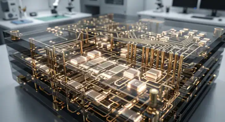
An HTCC vs LTCC ceramic PCB represents the two primary branches of co-fired ceramic technology, where HTCC stands for High-Temperature Co-Fired Ceramic, and LTCC stands for Low-Temperature Co-Fired Ceramic. Unlike DBC or DPC processes which apply metal to a pre-fired rigid ceramic plate, co-fired technology prints conductive paste onto flexible, unfired “green tape” layers, stacking and firing the entire 20 to 50-layer structure simultaneously in a kiln.
Why does the co-fired distinction matter? Because the ceramic and the metal must shrink together during the firing process, the materials are locked into specific pairings. You cannot put low-melting-point copper into a 1500°C HTCC furnace, just as you cannot expect an LTCC substrate filled with low-melting glass to survive extreme mechanical shocks like a pure alumina board.
- Co-Fired Process: Unfired ceramic tape and metal paste are baked together at the same time.
- Non-Co-Fired (DBC/DPC): Metal is bonded to a ceramic board that has already been hard-fired.
- Layer Count: Both HTCC and LTCC easily support 20 to 50 layer dense interconnects.
| Feature | HTCC Ceramic PCB | LTCC Ceramic PCB | Non-Co-Fired (DBC/DPC) |
|---|---|---|---|
| Manufacturing State | Co-fired (Green tape) | Co-fired (Green tape) | Post-fired metallization |
| Maximum Layers | 20 – 50+ | 20 – 50+ | Typically 1 – 2 (up to 4) |
| Core Advantage | Extreme physical strength | Embedded passives / RF | Extreme heat dissipation |
Choose HTCC or LTCC only when your design strictly requires massive 20+ layer interconnect density in a microscopic package. Avoid co-fired technologies entirely if your design only needs 1 to 2 layers, as DBC or DPC will be significantly cheaper.
Bottom line: HTCC and LTCC exist specifically to build ultra-dense, 3D multilayer structures that standard pre-fired ceramic boards physically cannot achieve.
What Is the Firing Temperature Difference and Why Does It Matter?
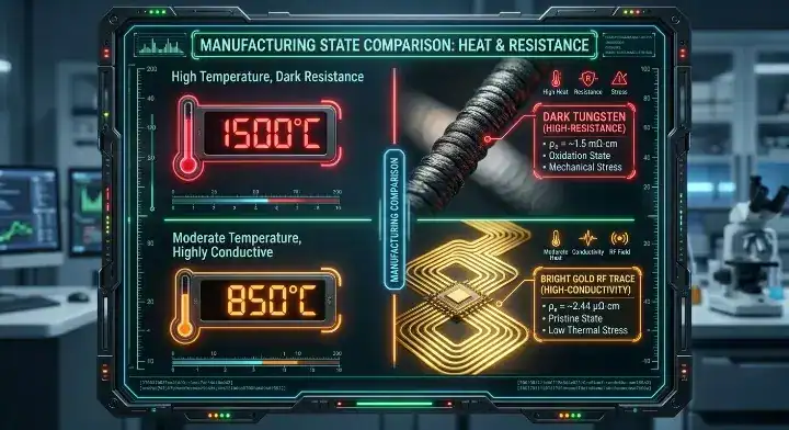
The defining specification of an HTCC vs LTCC ceramic PCB is the kiln temperature; HTCC requires extreme firing at 1300–1600°C to fuse pure alumina or aluminum nitride, whereas LTCC adds 30% to 50% glass frit to the ceramic matrix, artificially lowering the required firing temperature to a manageable 850–950°C. This temperature drop dictates every subsequent electrical and thermal property of the board.
What does this mean for your design? The high firing temperature of HTCC burns out all impurities, resulting in an incredibly dense, rock-hard substrate with zero porosity. The low firing temperature of LTCC saves energy and allows for better conductors, but leaves the final board mechanically weaker and packed with thermally insulating glass.
- HTCC Firing: 1300–1600°C (Requires specialized high-temp kilns).
- LTCC Firing: 850–950°C (Enabled by glass additives acting as a flux).
- Physical Hardness: HTCC is significantly harder and more brittle than glass-filled LTCC.
Bottom line: The firing temperature strictly controls the material chemistry; you accept the glass-filled weakness of LTCC specifically to gain access to low-temperature, high-conductivity metal routing.
Which Conductor Materials Can Each Process Use?
Because of its extreme firing temperature, an HTCC ceramic PCB forces engineers to use refractory metals like Tungsten (W) or Molybdenum (Mo) which only possess 20% to 30% of the electrical conductivity of copper. Conversely, an LTCC ceramic PCB fires below 1000°C, allowing the use of highly conductive Gold (Au), Silver (Ag), or Copper (Cu) pastes without melting them in the furnace.
Why is this a severe limitation for HTCC? Tungsten is a terrible conductor for high-frequency signals. When you push a 5 GHz signal through a tungsten trace on an HTCC board, the resistance and skin-effect losses are massive. LTCC solves this completely by using pure silver or gold, making it the undisputed champion for millimeter-wave routing. Following proper ceramic PCB RF layout rules requires matching your frequency to the correct conductor metal.
- HTCC Conductors: Tungsten (W), Molybdenum (Mo), Mo-Mn (High resistance).
- LTCC Conductors: Silver (Ag), Gold (Au), Copper (Cu) (Low resistance).
- RF Performance: LTCC conductors transmit GHz signals with near-zero resistive loss.
| Substrate | Typical Conductor | Electrical Conductivity | High-Frequency Suitability |
|---|---|---|---|
| HTCC | Tungsten (W) | ~30% IACS | Poor (High insertion loss) |
| LTCC | Silver (Ag) | ~105% IACS | Excellent (Low insertion loss) |
| DPC | Pure Copper (Cu) | 100% IACS | Excellent (Surface routing only) |
Choose LTCC when routing high-frequency RF signals because its silver/gold conductors prevent massive signal loss. Avoid HTCC for gigahertz applications as the tungsten traces will severely degrade your signal integrity.
Bottom line: HTCC sacrifices electrical conductivity to survive the furnace; LTCC lowers the furnace temperature specifically to use superior RF-friendly metals.
How Do Thermal Conductivity and Hermeticity Compare?
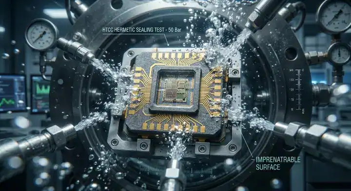
The thermal conductivity of an HTCC ceramic PCB sits at a respectable 16–17 W/m·K (using Al₂O₃), while an LTCC ceramic PCB drops to a disastrous 2–5 W/m·K due to its heavy glass content, making LTCC useless for high-power heat dissipation. However, HTCC provides absolute hermeticity (moisture and gas sealing), which allows it to pass strict MIL-STD-883 leak tests that LTCC often struggles with.
Engineers on the EEVBlog forum frequently run into this trap: “I am designing a power amplifier module running at 85°C ambient. A supplier recommended LTCC for the RF layers, but the datasheet says thermal conductivity is only 3 W/m·K. Is that enough?” The hard truth is no. At 85°C ambient, a high-power amplifier requires aggressive heat spreading to prevent the junction temperature from exceeding 150°C. A 3 W/m·K LTCC board acts as a thermal blanket, baking the chip to death. If you need multilayer RF routing plus heavy heat dissipation, you must pivot. We route the RF on top layers but use a non-co-fired DPC AlN base (150–170 W/m·K) to sink the heat. According to IPC (ipc.org) standards, IPC-6012 Class 3 dictates high-reliability layer registration within ±25 μm, meaning hybrid stacks must be manufactured perfectly. Reviewing our guide on power module substrate selection will save your thermal architecture.
- HTCC Thermal Conductivity: 16–17 W/m·K (Al₂O₃) / Up to 170 W/m·K (AlN).
- LTCC Thermal Conductivity: 2–5 W/m·K (Glass-ceramic composite).
- Hermeticity Definition: The ability to completely block moisture and gas penetration in a vacuum.
| Feature | HTCC Ceramic | LTCC Ceramic | DPC AlN (Non-Co-Fired) |
|---|---|---|---|
| Thermal Conductivity | 16 – 17 W/m·K | 2 – 5 W/m·K | 150 – 170 W/m·K |
| Hermetic Sealing | Excellent (MIL-STD-883) | Poor to Fair | Not Applicable (Bare board) |
| Best Use Case | Military sealed packages | Low-power 5G RF modules | High-power IGBT/SiC |
Choose HTCC if your component must survive decades in space or deep underground without moisture ingress. Choose a DPC AlN board immediately if you need to dissipate more than 5W of heat from an amplifier.
Bottom line: Never use LTCC for power electronics; its glass content turns it into a thermal insulator, guaranteeing your high-power chips will overheat.
Can LTCC Embed Passive Components — and What Does That Mean for Your Design?
Yes, a massive advantage of an LTCC ceramic PCB is its ability to embed passive components directly into the inner layers by printing dielectric and resistive pastes onto the green tape before firing. Because HTCC fires at 1500°C, the resistive pastes would simply burn away, meaning HTCC cannot embed passive components internally.
Why does embedding matter for 5G? When you embed dozens of capacitors and resistors into the LTCC substrate, you eliminate the need to solder surface-mount (SMD) components. This shrinks the overall package volume by 40% to 60%, removes the parasitic inductance caused by solder joints, and creates the ultra-compact 3D antenna-in-package (AiP) structures required for modern smartphones and radar systems.
- LTCC Embeds: Resistors, capacitors, and complex inductors.
- HTCC Embeds: Cannot embed passives (Temperatures are too high).
- Benefit: Drastically reduces external BOM count and shrinks the footprint.
Bottom line: If your design requires shrinking a complex RF front-end module by burying dozens of passive components inside the board, LTCC is the only viable technology.
What Are the Real-World Applications for HTCC vs LTCC?
The primary application for an HTCC ceramic PCB is military and aerospace hermetic packaging (like missile guidance sensors), whereas an LTCC ceramic PCB completely dominates the commercial 5G millimeter-wave and automotive radar markets due to its superior RF characteristics. According to Electronic Design (electronicdesign.com), LTCC’s low dielectric constant ($\varepsilon_r \approx 5-8$) and ultra-low loss tangent ($\tan\delta \approx 0.001-0.003$) make it the absolute standard for compact RF front-end modules.
Users on Reddit’s r/PrintedCircuitBoard often ask: “Military suppliers quoted me HTCC for an industrial sensor, but it is 10 times the price of a standard ceramic board. Do I really need HTCC?” Here is where engineers waste money. A defense contractor came to us needing a substrate for a downhole sensor rated to 175°C continuous operation. Their initial spec called for HTCC based on a prior vendor’s recommendation. After reviewing the actual requirements, we realized they needed electrical insulation, 150°C+ operational temperature, and moisture resistance, but NOT true hermetic sealing (MIL-STD-883). We proposed a DPC AlN substrate instead. DPC AlN delivers 150–170 W/m·K thermal conductivity, easily handles 175°C environments, and passed the vibration tests perfectly. The total substrate cost came in at 22% of the HTCC quote. The client has now standardized on DPC AlN for all their non-hermetic high-temperature designs.
- HTCC Applications: Deep space satellites, missile guidance, downhole oil drilling.
- LTCC Applications: 5G smartphones, 77 GHz automotive radar, Bluetooth modules.
- DPC Applications: EV traction inverters, high-power industrial LEDs.
| Market Sector | Primary Requirement | Recommended Technology |
|---|---|---|
| Aerospace & Defense | Hermetic sealing, physical strength | HTCC |
| Telecom & Automotive | 5G RF routing, 77 GHz radar, small size | LTCC |
| Industrial Automation | High heat dissipation, non-hermetic | DPC / DBC |
Choose HTCC only if the specification sheet legally mandates MIL-STD-883 hermetic sealing. Avoid HTCC for standard industrial projects, as the 10x cost premium provides zero measurable benefit over DPC.
Bottom line: HTCC is an extremely expensive niche process for military hermeticity; for commercial RF use LTCC, and for commercial power use DPC.
How Do Cost and Lead Time Compare at Prototype vs Production Scale?
At production volume, an HTCC ceramic PCB costs roughly 3 to 8 times more than an equivalent LTCC ceramic PCB because the tungsten metallization, 1500°C specialized kilns, and slower firing cycles drive massive overhead costs. Furthermore, both co-fired processes require expensive hard tooling and punching dies for the green tape vias, making prototype NRE (Non-Recurring Engineering) exceptionally high compared to standard ceramic boards.
We deal with these timelines daily: We quote HTCC and LTCC projects occasionally, but they always come with a frank conversation about lead time. A standard RF PCB manufacturing run for a DPC ceramic prototype takes 10–15 business days from our facility. HTCC substrates from qualified co-fired foundries typically take 35–55 days for custom prototypes because the green tape preparation, layer registration, and high-temperature kiln scheduling all add up. LTCC is slightly faster—25–40 days—because 850°C firing cycles are shorter. When clients ask us to compare HTCC/LTCC versus DPC for a multilayer power application, we almost always find DPC multilayer is the better call: same layer count, thermal conductivity 4–8x higher than LTCC, 30–50% lower cost, and 2–3 weeks faster delivery.
- Prototype (5–10 pcs): HTCC takes 35–55 days; LTCC takes 25–40 days.
- Mid-volume (100–500 pcs): HTCC unit cost is 3–8x higher than LTCC.
- High-volume (1,000+ pcs): DPC/DBC remains 80% cheaper than HTCC for non-hermetic needs.
Bottom line: Co-fired technologies are slow and expensive to prototype; never specify HTCC or LTCC unless your design strictly requires 20+ layers or military-grade hermeticity.
What Are the Most Frequently Asked Questions About Co-Fired Substrates?
What is the main difference between HTCC and LTCC ceramic PCB? HTCC fires at 1300–1600°C using tungsten or molybdenum conductors, producing hermetic, high-strength substrates for military and aerospace use. LTCC fires at 850–950°C using gold or silver conductors, allowing embedded passive components and superior RF performance. HTCC costs 3–8x more than LTCC for equivalent layer counts.
Is LTCC good for high-power applications? No. LTCC thermal conductivity is only 2–5 W/m·K because the glass additives that enable low-temperature firing also reduce heat transfer. For power applications above 5W, DBC or DPC ceramic substrates with 20–170 W/m·K thermal conductivity are far more suitable.
Which ceramic PCB process is best for 5G RF modules? LTCC is the standard choice for 5G RF front-end modules. Its low dielectric constant ($\varepsilon_r \approx 5-8$), low loss tangent ($\tan\delta \approx 0.001-0.003$), and ability to embed passive components in a multilayer 3D structure make it the dominant technology for millimeter-wave antenna-in-package designs.
Choosing between HTCC and LTCC dictates whether your module survives extreme military conditions or successfully routes gigahertz telecom signals. We understand that navigating the cost premiums and lead times of co-fired foundries is a high-risk process. At QueenEMS, we bypass the confusion by analyzing your actual thermal, RF, and hermetic requirements before production begins. If you are unsure whether your design warrants an expensive HTCC upgrade or if a standard DPC board will suffice, contact us to schedule a free DFM review today.
Written by the QueenEMS Engineering Team
Upload your files today · Free DFM check before production · Ship worldwide
Get your PCB prototypes in as fast as 24 hours. We handle FR4, Rogers, and Flex up to 60 layers — free prototypes for 2–4 layer boards, no minimum order.
Just upload your Gerber + BOM — we source every part, assemble, and inspect (AOI + X‑Ray) so you don't have to chase suppliers. Boards ship in as fast as 24 hours.