

Quick Answer: Order a Taconic RF-35 PCB against the exact standard grade, applicable manufacturer documentation, approved dielectric and copper construction, and agreed inspection scope. RF-35TC, RF-35HTC and RF-35P require separate approval. Keep historical typical values tied to their test conditions, resolve material availability before releasing tooling, and define which delivery records establish material identity, finished geometry and any required RF performance.
A fabrication offer can name Taconic RF-35 and still leave the build uncertain. The drawing may specify a dielectric thickness while the quotation lists finished board thickness. A supplier may suggest a related grade, or attach a property table whose test frequency differs from the design model. Those details belong in the order review before artwork and inspection requirements are frozen.
The standard RF-35 documents cited here are archival Taconic originals. They explain the material and several manufacturing concerns, but current availability and the documentation applicable to a particular purchase need supplier confirmation. This guide turns that evidence into questions an RF engineer, purchasing buyer and quality reviewer can resolve together.
Table of Contents
- Identify standard RF-35 before accepting the offer
- Keep each material value attached to its test condition
- Specify dielectric height and the complete copper construction
- Plan RF-35 registration around the actual panel
- Review drilled RF-35 features by their finished function
- Preserve the etched substrate for bonding and solder mask
- Define every interface in an RF-35 multilayer build
- Freeze the final conductor, mask and finish boundaries
- Match delivery evidence to the claim being accepted
- Release a repeatable RF-35 fabrication package
Identify standard RF-35 before accepting the offer
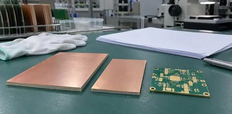
Specify the full RF-35 designation and require the supplier to identify the offered material before accepting a fabrication quote. A family name or shared nominal dielectric constant cannot establish an approved substitute.
Taconic’s archived RF-35 data sheet describes an organic-ceramic laminate with woven-glass reinforcement and PTFE, or polytetrafluoroethylene. This construction differs from a solid ceramic circuit substrate. The manufacturer identity also needs a current reference: AGC identifies AMMK as the former Korea Taconic, with the company name changed in May 2024.
| Name appearing in the offer | What the reviewer should resolve | Order action |
|---|---|---|
| Standard RF-35 | Exact laminate designation, source, document revision and ordered form | Match the drawing and material record |
| RF-35P | A separate woven-glass construction described in the historical processing guide | Review the proposed change before release |
| RF-35TC | A separate thermally conductive grade in AGC’s product range | Request its own documentation and engineering approval |
| RF-35HTC | A separate grade that AGC describes as non-reinforced | Review mechanical and fabrication assumptions as well as electrical ones |
| “RF-35 equivalent” | Exact replacement code and changes to construction or model inputs | Keep the alternate pending until approval is recorded |
The grade distinction is visible in AGC’s separate RF-35TC and RF-35HTC product descriptions. Their properties must stay attached to those names.
For an illustrative document review, suppose the drawing specifies RF-35 but the offer lists RF-35TC. Ask for a corrected offer or an explicit alternate proposal with the design impact identified. Use the established material substitution approval process to record that decision before the material is purchased.
Keep each material value attached to its test condition
An RF-35 property value needs its document, frequency, method and value type beside it. Preserve those conditions when reviewing design assumptions or supplier literature.
Read the archived table with its frequency
The historical Taconic RF-35 typical-values page, marked 2/02, lists dielectric constant, Dk, of 3.50 and dissipation factor, Df, of 0.0018 at 1.9 GHz, with IPC-TM-650 2.5.5 identified as the test method. It also states that reported typical values should not be used as specification limits. These are historical reference values, not a verified current shipment specification.
A copied table can lose its frequency heading when pasted into a quotation. If 0.0018 appears alongside a 10 GHz design requirement, the reviewer should recover the source before accepting the comparison. Relabeling the historical value does not create a 10 GHz measurement.
| RF-35 reference encountered | Condition the record must preserve | Decision it can support |
|---|---|---|
| Archived Dk 3.50 / Df 0.0018 table | Typical values at 1.9 GHz; page marked 2/02 | Identify the historical design reference |
| AGC slash-sheet grouping | Nominal Dk, material designation and document edition | Check category correspondence |
| Supplier-issued material specification | Exact grade, applicable limits, method and revision | Agree the purchased material requirement |
| Designer’s RF model | Selected dielectric value, frequency and construction assumptions | Review the modeled circuit geometry |
Separate model inputs from acceptance limits
Three records serve different jobs: the supplier’s applicable material specification, the designer’s dielectric model and the finished board acceptance plan. Identify the source used in each. A field solver may use a design-specific effective value, while a purchased laminate is controlled against an agreed specification and test method.
AGC’s July 2025 IPC slash-sheet reference lists RF-35 with nominal Dk 3.50 in its IPC-4103B/240 grouping. That reference helps identify the material category; it does not make every grade in the group interchangeable or certify the proposed sheet.
When source values differ, return the unresolved condition to the engineer responsible for the model. The purchase package should record which document applies and which finished-board result must be checked, so receiving inspection has a defined acceptance basis.

Specify dielectric height and the complete copper construction
Call out the RF-35 dielectric thickness separately from the finished board thickness, copper cladding, deposited copper and surface finish. Each belongs to a different part of the construction.
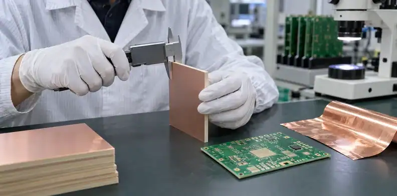
For a microstrip path, the conductor-to-reference-plane dielectric height is a design input. For a connector or enclosure, overall finished thickness may determine mechanical fit. A single thickness entry in a quotation can leave one of those requirements unresolved. The historical RF-35 order form treats laminate thickness and copper cladding as separate choices; current purchasable forms still need confirmation.
| Construction field | Information to put in the released stackup | Why it affects the RF-35 order |
|---|---|---|
| RF-35 core | Dielectric thickness and its agreed tolerance | Establishes the RF layer’s reference spacing |
| Copper on each face | Foil designation, nominal starting weight and applicable profile information | Names the supplied cladding |
| Added copper | Which surfaces and holes receive plating; finished requirement | Separates starting foil from final conductor geometry |
| Bonding layer, if used | Exact material and expected pressed thickness | Defines the dielectric outside the RF-35 core |
| Finished board | Overall thickness, measurement condition and tolerance | Controls installed fit and receiving inspection |
Consider an illustrative thickness calculation. A 20 mil dielectric is 0.508 mm. If the assumed starting copper is 35 µm on each face, the total is 0.578 mm before any added plating, finish or mask. Those assumptions describe an example, not an offered RF-35 product or a finished tolerance.
If the same drawing also demands a 0.508 mm finished board, engineering must resolve the two callouts. Ask the supplier to return a proposed stackup that identifies the measurement boundaries, then record the approved construction through supplier stackup signoff. Freeze that stackup before authorizing impedance-related geometry changes.
Plan RF-35 registration around the actual panel
Use construction-specific fabrication data to plan registration and artwork compensation. A published dimensional-change range is a reference for review, not a scaling instruction for every RF-35 panel.
A worked dimensional-change review
The Taconic RF-35/RF-35P processing guide gives a reference dimensional-change range of 200–400 parts per million and explains that movement depends on thickness, glass style, construction, foil and circuit pattern. It recommends determining compensation from fabrication samples or relevant experience.
For a worked engineering example, assume a 100 mm feature span and 300 ppm movement. The magnitude is 100 × 300 / 1,000,000 = 0.030 mm. This calculation gives the reviewer a scale to investigate. It does not predict the direction of movement, the behavior of an actual lot or the correct CAM compensation.
A useful verification trial tracks selected fiducials and critical features through the relevant process stages on the proposed panel. Compare the results with the drawing’s registration budget. Preserve the panel construction and measurement references with the result so a later production lot can be reviewed against the same baseline.
Authorize geometry adjustments before tooling
Different RF features need different review boundaries. A transmission-line width, a coupled-line gap and a connector launch may each affect the circuit response. The fabricator needs to know which dimensions may be adjusted to meet an agreed target and which require design approval.
In an illustrative filter-board review, suppose a proposed etch adjustment changes both conductor width and coupling gap. The RF engineer should review both changes together before CAM release. A favorable impedance prediction for one line does not settle the filter’s coupling geometry.
Keep the released artwork, approved adjustments and panel measurement record together. These provide a repeat-order reference without treating the historical dimensional-change range as measured production capability.

Review drilled RF-35 features by their finished function
Review holes in standard RF-35 according to what each finished feature must do. A plated via, a connector lead hole and a mechanical opening have different acceptance questions.
The historical processing guide identifies RF-35’s 7628 woven-glass reinforcement and describes fiber protrusions that can occur during drilling. It also distinguishes these from resin smear and hole-wall damage. This is a reason to ask for a qualified drilling route for the proposed construction, not to copy a feed, speed or tool-life limit into the purchase order.
| RF-35 feature | Functional question | Evidence to agree before fabrication |
|---|---|---|
| Plated signal or ground via | Is the required conductive structure continuous and acceptably formed? | Finished-hole and interface inspection tied to the relevant hole family |
| Plated connector lead hole | Will the specified lead fit the finished opening after plating? | Finished bore requirement, applicable fit check and hole-quality evidence |
| Unplated locating or mounting hole | Does the opening meet its mechanical purpose? | Dimensional and edge-condition inspection against the drawing |
| Hole crossing an RF-35 bond interface | Is the process suitable for all materials encountered? | Construction-specific process review and the agreed cross-section locations |
A connector prototype offers a practical example. An electrical continuity result can establish a conductive connection, yet the receiving team may still need a defined lead-fit check. State the finished condition being measured so an inspection of the pre-plated opening is not accepted as the final fit result.
Keep the RF-35 material identity on the drill-path review. If RF-35P is proposed to change drilling behavior, the decision returns to material approval. The broader PTFE hole preparation evidence requirements explain activation and metallization controls; this order should apply them to its specific RF-35 hole families.

Preserve the etched substrate for bonding and solder mask
Agree how the exposed RF-35 substrate will be handled and prepared between etching, bonding and solder-mask application. Surface condition is part of the fabrication route.
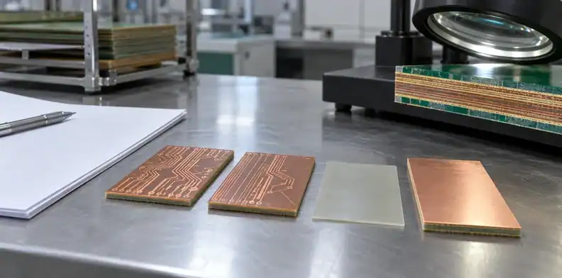
The Taconic processing guide explains that the treated copper leaves an imprint in the PTFE surface after etching. Mechanical abrasion can disturb that surface and affect subsequent bonding. It also cautions against handling that bends or dents panels. These historical mechanisms help frame the process review; the supplier must qualify the route used with the actual material and mask system.
An RF-35 board with large exposed dielectric areas makes the handling question visible. Ask how the panel is supported during inspection and transport between processes, and how debris or fingerprints are prevented from reaching surfaces that will be bonded or coated. The response should identify the applicable handling and surface-preparation controls.
For a multilayer core, a sample of etched dielectric can help review the proposed preparation sequence. For a masked two-layer board, agree what adhesion evidence applies to the selected mask and substrate. These checks concern different interfaces, so identify the tested surface and processing stage in the report.
A photograph can show panel handling or surface damage, but material identity comes from traceable records. Link the inspection sample to the RF-35 lot and construction used in the trial before relying on it for production release.

Define every interface in an RF-35 multilayer build
Specify the RF-35 core and every adjacent bonding or dielectric layer separately. The finished multilayer stack needs its own construction review, even when a two-layer RF-35 prototype has performed satisfactorily.
Show the RF-35 core and bondline separately
The words “RF-35 multilayer” leave the bonding system open. Mark the RF-35 layer locations, copper faces, adjacent cores and bonding materials on the proposed stackup. Identify which dielectric layers enter the RF model and which holes cross each interface.
If a design combines an RF-35 section with another laminate system, ask for the reviewed material combination and expected pressed geometry. The existing hybrid lamination review covers the general compatibility assessment. The RF-35 order should add the exact core and its interfaces to that assessment, with any unapproved alternate shown separately.
Carry the assembly exposure into qualification
The board will also see assembly and possibly rework. AGC’s manufacturer Q&A explains that warpage and rework behavior depend on construction and processing conditions. A material property table alone cannot define the allowable history for the assembled product.
Provide the intended soldering and rework exposures to the qualification reviewer. Agree whether the first-article evaluation includes measurements after those exposures and who performs them. A bare-board report should identify its inspection state clearly; later assembly qualification needs its own evidence and responsibility.
Freeze the final conductor, mask and finish boundaries
Describe the finished RF copper, solder-mask coverage and surface-finish regions in the fabrication package. The construction being accepted should match the one used for the RF design and prototype review.
Start with the reference plane and RF layer identified on the stackup. Then define the conductor geometry, the permitted adjustment process and the surfaces receiving deposited metal. Starting foil weight does not describe every finished copper feature after pattern plating. Keep the associated geometry requirements in the drawing or approved CAM response.
Copper profile is another material input that needs an identified source. If a proposed change modifies foil type or treatment, review its electrical and fabrication implications before approval. The copper foil profile purchasing guide provides the broader selection framework; an RF-35 order must still confirm the actual cladding offered.
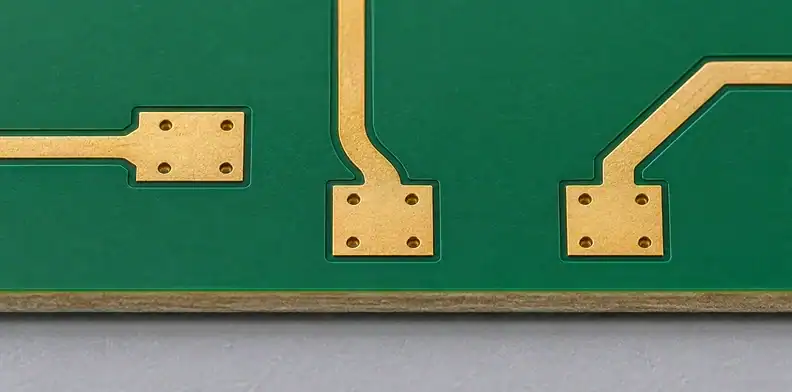
Show mask openings and exposed conductor regions explicitly. For example, a prototype antenna with an exposed feed region should carry that coverage boundary into the production files. A mask added across the feed region introduces a construction change for the engineer to review.
Also identify the required finish on soldering, contact or bonding areas. The supplier needs enough information to quote the intended surface definition and any special processing. Record the final boundaries before RF validation so a later production inspection can check the same geometry and coverage.
Match delivery evidence to the claim being accepted
Agree the delivery evidence by acceptance question. Material traceability, physical inspection, netlist testing, impedance measurement and RF performance evaluation establish different parts of an RF-35 build.
| Acceptance question | Evidence to request | Scope to check on the returned record |
|---|---|---|
| Was the specified standard RF-35 used? | Material identification and traceability records | Grade, source, lot and applicable document correspondence |
| Was the agreed construction fabricated? | Released stackup and dimensional or cross-section records | Measured locations, dielectric/copper boundaries and drawing revision |
| Are the required nets connected and isolated? | Bare-board electrical test record | Tested netlist and accepted board revision |
| Does the selected structure meet its impedance target? | Defined coupon and impedance report | Coupon geometry, measurement conditions and acceptance limit |
| Does an RF path meet its loss or phase requirement? | Agreed RF coupon or product evaluation | Frequency range, fixture/reference planes, method and limits |
For physical evidence, use the microsection report review to check whether the chosen cut location addresses the feature of concern. A convenient cross-section of a different hole or layer interface may leave the RF-35 question open.
An impedance report needs its own coupon and result references. If the project also requires insertion-loss or phase measurements, include that scope in the quotation. The established loss-coupon RFQ planning section explains the inputs needed to make that request reviewable.
For a filter pilot, the buyer might accept bare-board fabrication against dimensional, netlist and material requirements while the engineering team separately evaluates the assembled filter response. Record both responsibilities. This keeps a successful bare-board inspection from being reported as a completed product-level RF qualification.
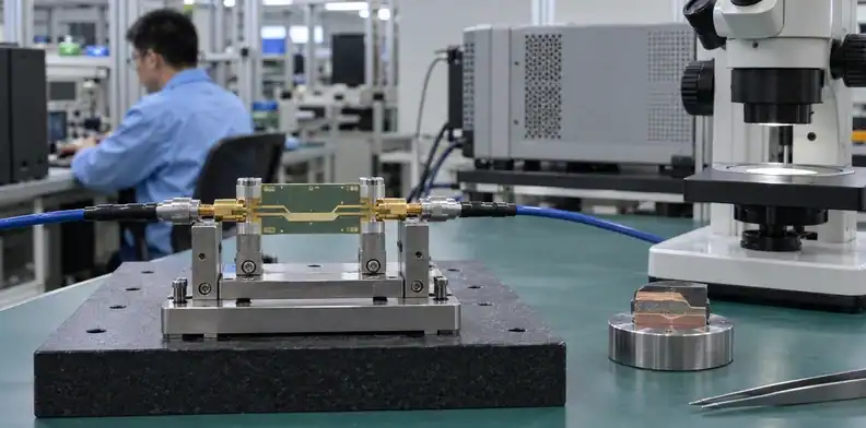
Release a repeatable RF-35 fabrication package
Release an RF-35 order when the offered grade, construction, approved adjustments and evidence scope agree across the drawing, quotation and inspection plan. Carry the accepted first-article baseline into repeat orders.
A useful RF-35 request for quotation includes:
- Current fabrication data and drawing revision, with the exact standard RF-35 callout.
- Applicable manufacturer documentation and the rule for proposed substitutions.
- Approved layer construction, dielectric heights, copper cladding and finished thickness.
- Critical RF dimensions and the permissions governing CAM adjustments.
- Finished hole functions, mask boundaries, finish regions and mechanical requirements.
- Quantity, panel or delivery format, required reports and any separate RF validation scope.
- Intended assembly exposure where it affects the qualification request.
Keep open decisions visible in the supplier’s response. A quotation based on confirmed standard RF-35 and a released stackup can be reviewed directly. An offer based on an alternate grade or an unresolved thickness should state those assumptions and identify what must be approved before release.
After the pilot, preserve the accepted material record, stackup, CAM revision, coupon references and inspection results. Ask how the supplier will notify you of changes to that baseline before a repeat build. This gives engineering a concrete basis for deciding whether a change needs document review, additional coupons or another product evaluation.
Use the agreed shipment documentation requirements to specify the records returned with production. For an RF-35 fabrication review, send QueenEMS the current drawing, construction and open material questions, including the evidence you require before accepting the boards.
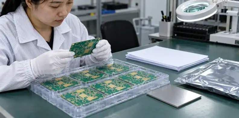
Sources
- Taconic RF-35 archival data sheet, typical-values page marked 2/02, hosted by NETSKET.
- AGC July 2025 IPC slash-sheet reference.
Written by the QueenEMS Engineering Team.
Upload your files today · Free DFM check before production · Ship worldwide
Get your PCB prototypes in as fast as 24 hours. We handle FR4, Rogers, and hybrid boards up to 40 layers in volume production, with advanced builds subject to engineering review — free prototypes for 2–4 layer FR-4 boards, no minimum order.
Just upload your Gerber + BOM — we source every part, assemble, and inspect (AOI + X‑Ray) so you don't have to chase suppliers. Boards ship in as fast as 24 hours.