
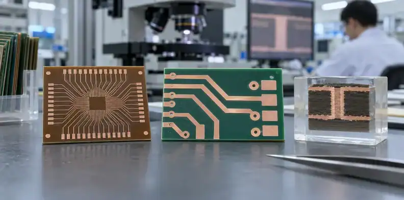
Quick Answer: An mSAP PCB process is worth reviewing when the required finished line and space cannot be produced consistently by the available subtractive route at the specified copper thickness. Compare mSAP with SAP using the actual layer construction, seed copper, imaging capability and inspection plan. Apply finer processing to the layers that need it, then verify the finished geometry and electrical performance before committing the construction to production.
A dense layout can leave engineering with two unattractive choices: add routing layers or reduce trace width beyond the fabricator’s accepted rules. Choosing an mSAP PCB route introduces a third option, but the decision needs more than a smaller number on a capability sheet. A line that fits in CAD still needs enough copper, controlled spacing, suitable materials and a manufacturing route that can be repeated.
Start with the particular escape channel that fails. Establish which layers carry that constraint, compare the available processes, and keep the electrical model tied to the proposed finished board. The discussion below concerns fine lines on a board-level PCB, where package fanout, reference planes and production inspection must work together.
Table of Contents
- What changes between subtractive, SAP and mSAP?
- Find the routing constraint before changing the process
- Assign fine-line processing to the layers that need it
- Specify finished line, space and copper together
- Check the dielectric, seed copper and resist as a set
- Keep short neck-downs inside the electrical budget
- Review microvias independently of the fine-line route
- Prove the patterned layer before it becomes hidden
- Qualify the production route after the first sample
- Request a route-specific quotation from QueenEMS
What changes between subtractive, SAP and mSAP?
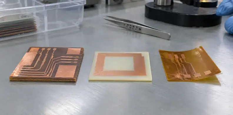
Subtractive processing forms circuits by removing unwanted copper; semi-additive processing forms the conductor through selective plating and removes the remaining thin conductive base between features. SAP and modified semi-additive processing, mSAP, differ in how that starting conductive layer is established.
High-density interconnect, or HDI, describes the interconnection construction. A board can combine HDI microvias with different circuit-forming processes. Keep the material and interconnection questions separate using the distinctions in BT package substrates versus board-level HDI.
| Circuit-forming route | Starting copper relevant to patterning | How the conductor is formed | What the supplier should identify |
|---|---|---|---|
| Subtractive | Copper-clad surface, potentially with prior plating | Protect the intended circuit and etch unwanted copper | Copper condition at etching and finished line/space envelope |
| SAP | Very thin deposited conductive seed on the dielectric | Plate the resist-defined pattern, strip resist and remove exposed seed | Seed method, dielectric preparation and accepted plating geometry |
| mSAP | Ultra-thin foil-based copper, with route-specific metallization | Plate the pattern and remove remaining thin base copper | Foil grade, starting copper condition and seed-removal allowance |
The table describes the circuit-patterning distinction rather than a complete traveler for every board. Via metallization and the order of build-up operations still depend on the chosen construction.
Mitsui Kinzoku’s MicroThin product documentation identifies carrier-supported copper foil designed for mSAP. Its ultra-thin copper and removable carrier are different physical layers. Neither the foil thickness nor the name of the process establishes the finished conductor height or a factory’s accepted minimum spacing.
Find the routing constraint before changing the process
Change the process only after locating a channel that cannot accommodate the required routes under the current manufacturing rules. Component pitch alone does not establish that a board needs SAP or mSAP; pads, capture lands, clearances and usable routing layers determine the available space.
Calculate the escape channel
Consider an illustrative layout with a clear corridor of 180 μm between copper obstacles. For n equal-width traces of width w, with equal spacing s between traces and at both boundaries, the required corridor is n × w + (n + 1) × s.
At hypothetical 50 μm lines and 50 μm spaces, one trace occupies 150 μm; two need 250 μm. With hypothetical 30 μm lines and 30 μm spaces, two occupy 150 μm, while three require 210 μm. Those dimensions are calculation inputs, not QueenEMS capability claims or process thresholds.
The smaller geometry fits two traces in this idealized corridor. It still needs a manufacturing feasibility check and an electrical review. A capture pad extending into the channel, a wider boundary clearance or a local registration requirement can remove the apparent advantage. Measure the corridor from the actual copper objects rather than deriving it from nominal package pitch.
Try the architectural alternatives
Compare the fine-line option with moving a component, changing the escape assignment, adjusting a permitted capture land or adding an approved routing layer. The fine-pitch BGA escape discussion addresses the fanout choices that precede this process decision.
For the example, send CAM a crop containing the obstacles and both candidate routes. Engineering should retain the route that meets clearance and signal requirements after the supplier applies its accepted finished-geometry rules. The calculation identifies a possible solution; it does not predict yield or prove the completed connection.

Assign fine-line processing to the layers that need it
A mixed stackup can use semi-additive signal layers alongside compatible subtractive layers. Select the route by layer, then let the fabricator confirm the complete construction and manufacturing sequence.
Altium’s technical discussion of SAP process combinations describes this approach and distinguishes it from switching between SAP and subtractive processing within one layer. A small dense region can require the whole layer to follow the fine-line patterning route; wider features elsewhere on that layer can use the same route.
| Illustrative layer function | Proposed patterning choice | Information that determines the choice |
|---|---|---|
| Top-side component escape | SAP or mSAP candidate | Dense escape geometry, pad clearance and finished copper |
| Inner signal layer with another tight channel | Separate fine-line assessment | Its own minimum spacing, dielectric and reference plane |
| Continuous reference plane | Conventional route candidate | Plane copper requirement and compatibility with adjacent build-up |
| Power distribution layer | Conventional route candidate | Required conductor section, current paths and connection method |
| Bottom-side signal layer without a dense region | Retain available route if adequate | Actual geometry and the approved overall fabrication sequence |
Use this functional map before fixing layer numbers. It avoids treating every layer as equally difficult while exposing combinations that the supplier must approve.
The HDI stackup architecture comparison covers the separate choice of build-up structure. Finer signal patterning may create routing options, but a claimed reduction in layer count needs a completed routing study. Record the proposed layer process in the stackup alongside dielectric thickness and copper requirements so the quotation describes one buildable board.
Specify finished line, space and copper together
An mSAP PCB quotation should bind line width and spacing to the finished copper height, measurement convention and layer location. A nominal artwork width or a best-case demonstration feature leaves those conditions unresolved.
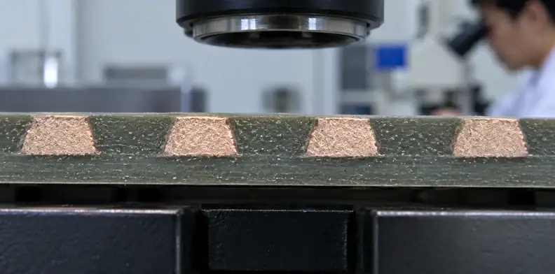
A conductor can have different top and base widths. Ask which width the quoted limit describes and how the agreed spacing will be measured. This prevents a narrow top measurement from being compared with a wider base dimension as though both results represented the same requirement.
| Geometry item | State it in the drawing or agreed attachment | Why it changes the process assessment |
|---|---|---|
| Finished line width | Nominal value, tolerance and measurement location | Establishes the copper feature being accepted |
| Finished spacing | Controlled edge-to-edge gap and affected nets | Connects isolation and route packing to the real conductor |
| Conductor height | Finished requirement for each fine-line layer | Links the narrow pattern to its electrical cross-section |
| Pattern extent | Short neck-down or repeated dense region, with coordinates | Distinguishes one local feature from a large patterned field |
| Pads and transitions | Land dimensions, joining geometry and permitted edits | Keeps process compensation from altering component escape |
After filling the table, compare the proposed dimensions with the original corridor calculation. A supplier’s finished spacing convention may require a different packing estimate.
QueenEMS’s fine-feature quotation evidence article covers the wider RFQ record. For a process change, add the supplier’s proposed route and its measurement basis to that record. Avoid specifying an unqualified smallest line together with a copper thickness borrowed from an unrelated conventional layer; request confirmation of the combined requirement.
Check the dielectric, seed copper and resist as a set
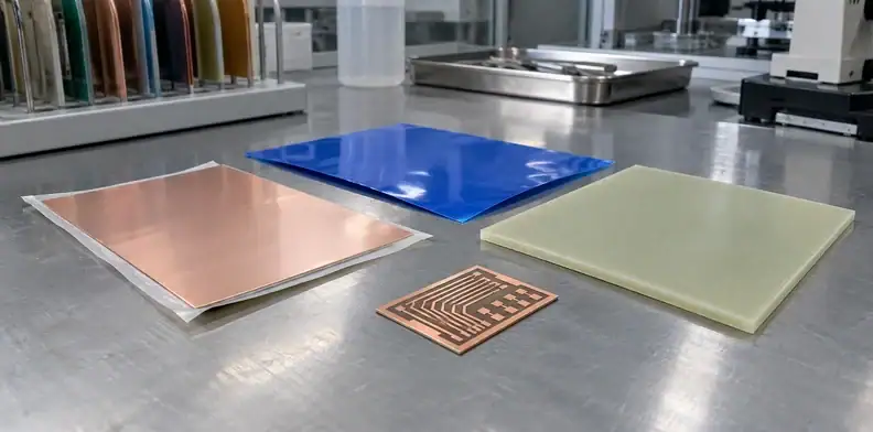
Evaluate the exact dielectric surface, conductive base and imaging material together. Evidence that a process works on one construction cannot establish the same geometry on a different surface or build-up material.
Separate seed foil from finished conductor
The removable carrier on an ultra-thin foil supports handling; it is not retained as the fine trace’s final copper thickness. Confirm the product grade and the point at which the carrier is removed. Deposited-seed routes instead need a defined preparation and metallization system for the dielectric.
A material change also needs review beyond its nominal dielectric constant. The HDI signal-speed material discussion covers the electrical material decision. The fine-line route adds surface preparation, adhesion and compatibility questions to that assessment.
Match imaging and adhesion to the surface
Qnity’s Riston Laser Series documentation separately reports design use and resolution after developing for its mSAP resist. A developed resist feature is an intermediate result. Plating, stripping and seed removal still have to produce the agreed finished copper.
The Atotech mSAP system description discusses desmear, electroless copper, electrolytic plating, particle control and uniformity. These are parts of an integrated manufacturing route, not evidence that QueenEMS owns that equipment.
Request a sample or coupon using the proposed dielectric and copper system. During qualification, assess the resulting conductor and its adhesion on that construction. An attractive resist image on another substrate cannot close the material decision.
Keep short neck-downs inside the electrical budget
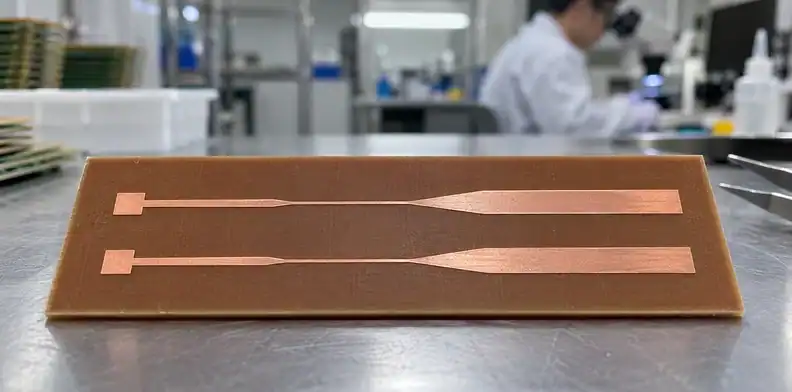
Use fine traces where routing needs them and check their length, conductor section and reference geometry against the electrical model. Smaller dimensions can solve a packing problem while creating a resistance, impedance or coupling problem.
Use the manufactured cross-section in the model
For a uniform conductor, DC resistance follows R = ρ × length / area. With the same copper resistivity, length and temperature, reducing the cross-sectional area increases resistance. This relationship provides a check on a proposed narrow route; it does not supply an ampacity limit or a high-frequency loss prediction.
Use the supplier’s proposed top width, base width and conductor height in the relevant model. Include the dielectric thickness and reference-plane arrangement. For high-speed nets, review the complete channel with the HDI high-speed layout considerations, rather than approving a fine trace because its cross-section looks rectangular.
Widen the route after the dense region
A local neck-down can join a wider conductor on the same patterned layer. Keep its extent visible in the routing file so the signal-integrity reviewer can assess the transition, length and neighboring conductors.
For a proposed differential pair, changing both trace width and spacing changes more than the corridor occupancy. The pair’s reference distance, coupling and transition geometry need review together. Confirm the coupon geometry and impedance target with the fabricator, then compare the agreed measurement with the design tolerance.
Power connections deserve their own copper section and thermal assessment. Do not propagate the smallest signal-routing rule into a current-carrying path merely because the fine-line process can pattern it.
Review microvias independently of the fine-line route
Fine-line patterning does not determine the microvia span, landing size, dielectric depth or acceptable via construction. Review these features separately even when the same manufacturing sequence plates traces and vias.
The layer-pair schedule should identify the source and target copper layers, via diameter, capture land and any fill or stacking requirement. Finer traces might pass between lands that previously blocked routing, but they cannot make a misregistered landing or an unsupported interconnection acceptable.
Cross-check that schedule with the HDI fabrication review topics. Keep the circuit-patterning decision beside the via decision in CAM correspondence. A proposal that narrows traces but also changes capture lands is a two-part engineering change.
IPC’s IPC-6012F release announcement identifies microsection evaluation and coupon designs for complex via structures among its expanded coverage. Agree the applicable specification, revision and construction-specific testing with the supplier. A fine-line surface sample cannot establish the reliability of a buried or stacked interconnection.
Stop release when the trace route is accepted but the proposed via construction remains outside the supplier’s confirmed scope.
Prove the patterned layer before it becomes hidden
Inspect the fine-line geometry while it is accessible, and agree how coupons or cross-sections will represent it after lamination. Electrical continuity, surface appearance and conductor dimensions answer different questions.
| Evidence | Fine-line question it can address | What remains outside that evidence |
|---|---|---|
| Calibrated top-view measurement | Width and visible gap at identified coordinates | Buried interfaces and conductor height |
| Pattern inspection or AOI record | Visible bridging, interruptions and local pattern defects within inspection capability | An independent proof of every finished dimension |
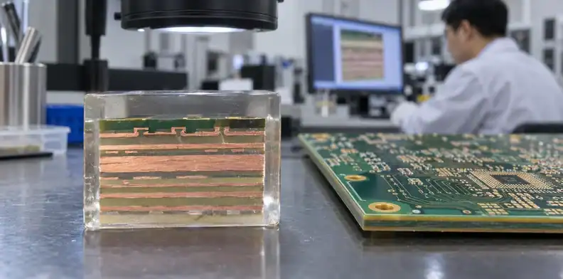
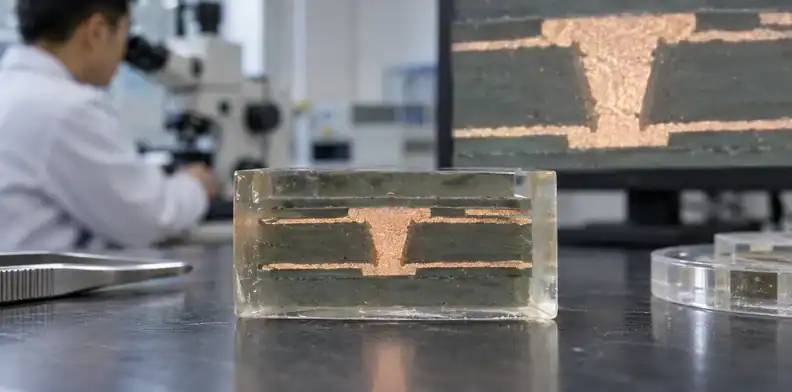
| Cross-section through a chosen feature | Conductor profile, height and a selected material interface | All locations across the production panel |
| Electrical test against the design netlist | Tested opens and unintended connections | The exact width of a conductor that still passes continuity |
| Relevant impedance coupon | Measured impedance of the agreed coupon construction | Every short neck-down and transition in the product |
Choose evidence for the defect or property that could invalidate the process selection. Avoid asking one report to establish everything in the table.
For hidden structure, the microsection report interpretation explains why location and construction identity belong beside the image. A fine-line cross-section should identify the layer, sample location, magnification or scale and the dimensions under review.
Agree representative locations in dense and less dense regions before the qualification panel is built. Request the intended measurement capability and acceptance method, especially where the feature is close to the quoted limit. Quality should know which dimensional or inspection result requires engineering disposition before the layer disappears into the stackup.
Qualify the production route after the first sample
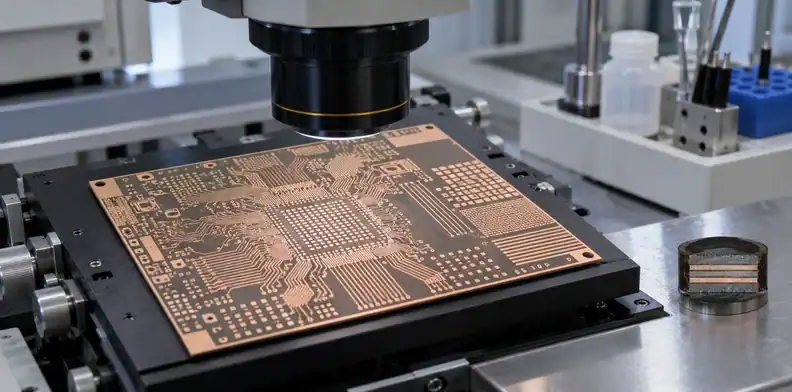
Treat an initial fine-line sample as a geometry demonstration. Production approval needs evidence that the proposed material, patterning and inspection route can reproduce the required features under the conditions intended for the order.
The INEMI laminates roadmap identifies adhesion, morphology, inspection and the transition from prototype processing to production as related challenges. It does not establish a universal qualification lot size or a guaranteed yield for a particular circuit process.
| Qualification stage | Fine-line result to establish | Condition that needs further work |
|---|---|---|
| Geometry demonstration | The specified conductor section and gap exist on the proposed construction | Sample uses another dielectric, relaxed dimensions or an unrecorded concession |
| Pilot panel | Agreed locations reproduce the dimensions and pass the chosen inspections | Only an easy isolated coupon was measured |
| Board evaluation | Electrical and assembly checks cover the released neck-downs and interconnections | Product tests rely on a materially different stackup |
| Production release | Process revision, inspection scope and permitted substitutions are defined | Factory proposes a route change without construction review |
Set the sample quantity, locations and test conditions according to project risk. The table separates the evidence questions; it is not a mandatory universal test protocol.
A repeat order should retain the accepted manufacturing interpretation. Use the processed CAM artwork approval discussion when compensation changes a controlled feature. A new foil grade, dielectric, finished copper requirement or manufacturing source can reopen the qualification question even when the nominal Gerber trace width stays the same.
For commercial comparison, request quotes on the same qualified route and inspection scope. Any expected reduction in routing layers or lamination cycles should appear in the proposed stackup; savings cannot be inferred from the mSAP label.
Request a route-specific quotation from QueenEMS
Submit the limiting routing geometry and ask QueenEMS to confirm the available manufacturing route before specifying SAP or mSAP as an assumed supply capability. The response should identify whether the released board can use an available subtractive route, requires geometry changes or needs a separately confirmed semi-additive construction.
Include the following process-selection inputs:
- The CAD routing crop showing the blocked channel, affected nets and required boundary clearance.
- A layer map identifying each fine-line region, its dielectric and its finished copper section.
- Fabrication data, drill spans and the proposed via construction, linked to one design revision.
- The neck-down lengths, controlled-impedance requirements and limits on permitted trace edits.
- Prototype and production quantities, qualification scope and the fine-line evidence required with the order.
Ucamco’s Gerber format information describes the format used to transfer PCB design data. Supply the fabrication files together with the construction notes; the artwork alone does not state the intended plating route or measurement agreement.
Ask for a clear feasibility disposition before relying on the quote’s delivery date. When a route cannot yet be confirmed, keep the proposed SAP/mSAP requirement open and identify the alternative that engineering will assess. Purchasing can then separate an order-ready board from a construction that still needs qualification.
For an mSAP PCB process review, send QueenEMS the route-selection package and request confirmation of the actual available process, the combined finished line/space/copper requirement and the quotation scope for representative verification. Include the subtractive alternative when one exists so engineering can compare both routes against the same routing constraint.
Sources
- Mitsui Kinzoku: MicroThin carrier-supported copper foil
- IPC: IPC-6012F construction and evaluation scope
Written by the QueenEMS Engineering Team
Upload your files today · Free DFM check before production · Ship worldwide
Get your PCB prototypes in as fast as 24 hours. We handle FR4, Rogers, and hybrid boards up to 40 layers in volume production, with advanced builds subject to engineering review — free prototypes for 2–4 layer FR-4 boards, no minimum order.
Just upload your Gerber + BOM — we source every part, assemble, and inspect (AOI + X‑Ray) so you don't have to chase suppliers. Boards ship in as fast as 24 hours.