
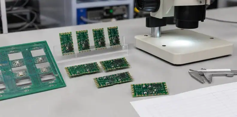
Quick Answer: Castellated hole plating acceptance should define the half-hole geometry, plated wrap, burr limit, pad exposure, solderability, and inspection evidence before module fabrication. Buyers should not treat castellations as ordinary routed slots because final routing can damage the plated barrel edge.
Castellated holes look simple on a finished module, but the process combines drilling, plating, routing through plated holes, edge quality, and solderable pad control. The risk is that the board passes electrical test while the half holes are hard to solder or inspect. This article is the acceptance-focused companion to the existing castellated requirements page. It helps buyers define what a finished castellated edge must prove before shipment.
Table of Contents
- What makes castellated hole acceptance different?
- Which geometry should be frozen before RFQ?
- How should burrs and copper tears be controlled?
- How does solder mask affect the half-hole pad?
- When is edge plating a related but separate issue?
- What shipment evidence should be requested?
- How should suppliers handle process changes?
- What should QueenEMS receive for castellated-hole review?
- How should castellated modules be released for repeat builds?
What makes castellated hole acceptance different?
Castellated hole acceptance is different because the finished feature is created by cutting through plated holes. That exposes a half barrel at the board edge, so plating continuity, burrs, copper pullback, and solderable geometry all become acceptance concerns.
Use PCB castellated holes requirements for the base design setup. This page focuses on what the buyer should inspect and request after the process is chosen.
Acceptance rule: judge the routed plated edge, not only the drilled hole size.
Which geometry should be frozen before RFQ?
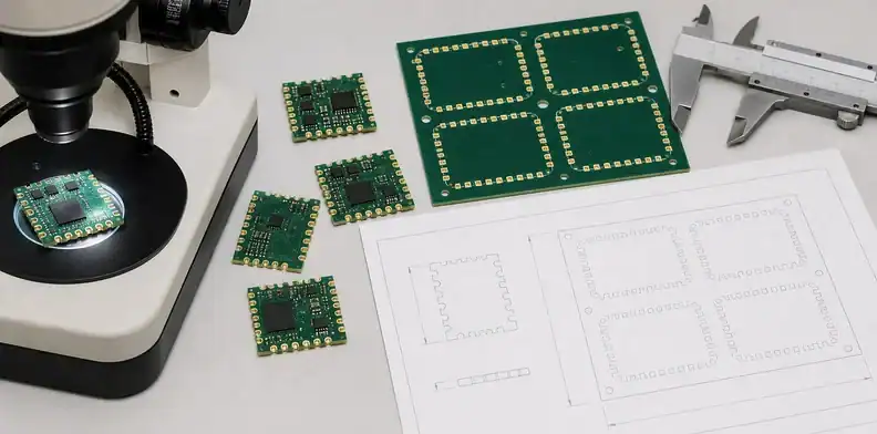
Freeze finished half-hole size, hole pitch, pad size, edge position, solder mask clearance, surface finish, board thickness, and the assembly mating method. The supplier needs to know whether the castellations support hand soldering, reflow, RF grounding, or module-to-carrier attachment.
Connect the drawing to PCB board outline tolerance because the routed edge location directly affects the remaining half-hole shape.
Geometry signal: quote castellations from finished edge geometry, not only drill coordinates.
| Drawing item | Why it matters | Buyer note |
|---|---|---|
| Hole pitch and diameter | Sets the module edge interface | Match the carrier-board footprint |
| Final route path | Creates the half-hole edge | Inspect after separation, not only before routing |
| Plating expectation | Controls solderable edge quality | Request photos or sample evidence when critical |
How should burrs and copper tears be controlled?
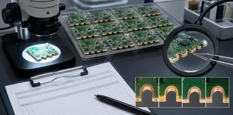
Burrs, copper tears, laminate breakout, and rough routed edges can make castellations hard to solder or visually unacceptable. The RFQ should state where burrs are rejectable and whether first-article photos are required for the edge.
The supplier may need a routing sequence, support tabs, or special handling to protect the plated edge. Ask for that assumption before awarding the order, especially for small modules with dense edge pads.
Edge rule: visible damage on the solderable half-hole edge needs a defined acceptance limit.
How does solder mask affect the half-hole pad?
Solder mask can encroach on the pad or leave too much exposed copper near the edge. The correct opening depends on how the module is soldered to the carrier board and whether visual fillets must be inspected.
Use PCB solder mask opening requirements when pad exposure is tight. The mask note should protect solderability without exposing unwanted copper around the module edge.
Mask call: castellated pad exposure should match the assembly and inspection method.
When is edge plating a related but separate issue?
Edge plating and castellations can appear on the same module, but they are not the same feature. Edge plating may support shielding or grounding along a continuous edge, while castellated holes create solderable half barrels.
When the design includes both, link the RFQ to PCB edge plating requirements and ask the supplier to separate the acceptance evidence for each feature.
Feature boundary: do not let an edge-plating note substitute for castellated-hole acceptance.
| Defect | Assembly concern | RFQ or acceptance action |
|---|---|---|
| Missing plating on the half hole | Weak solder fillet or open risk | Hold release for supplier disposition |
| Burr or chip at the edge | Fit and wetting concern | Inspect after depaneling |
| Irregular module outline | Carrier-board alignment issue | Compare to the assembly footprint |
What shipment evidence should be requested?
Shipment evidence can include first-article edge photos, visual inspection records, electrical test, solderability evidence when required, and any report identifying controlled castellated features. The evidence should show the actual routed half-hole edge.
Receiving can use PCB incoming inspection but should add a castellated-edge check for burrs, plating damage, missing wrap, and mask encroachment.
Proof rule: require evidence at the castellated edge, not only a general outgoing inspection label.
How should suppliers handle process changes?
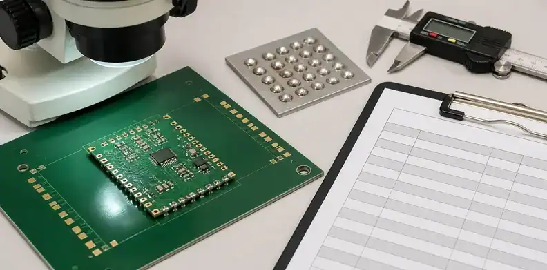
Supplier process changes may include drill size adjustment, pad resizing, routing path change, tab relocation, surface finish change, or solder mask relief. These changes can affect soldering and fit, so they need marked approval when the castellations are functional.
Ask the supplier to return a small marked review showing any proposed geometry or edge-processing change before CAM approval. That avoids discovering a different half-hole shape after the module arrives.
CAM boundary: any change that affects solderable half-hole geometry needs engineering approval.
What should QueenEMS receive for castellated-hole review?
QueenEMS should receive Gerber or ODB++ files, fabrication drawing, castellated-hole detail, assembly carrier information if available, surface finish, inspection expectations, and quantity. Send the package through the QueenEMS contact page so the review can separate hole geometry, edge quality, solderability, and evidence gaps before RFQ release.
A quote-ready package lets suppliers price the real module interface instead of treating castellations as ordinary drill and route work.
RFQ close: freeze the finished half-hole condition before supplier price becomes the baseline.
How should castellated modules be released for repeat builds?
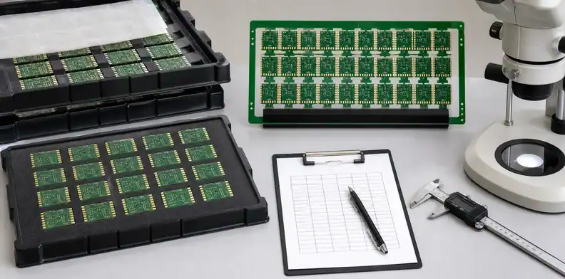
Castellated module release should preserve the finished edge condition, not only the drill file. The buyer should keep the accepted hole size, pad shape, routed edge location, surface finish, solder mask clearance, burr limit, and inspection evidence with the product revision. That information is what lets the module solder to the carrier board again.
A useful RFQ sentence is: “Castellated hole plating is controlled on the module edge. Supplier must confirm finished half-hole geometry, plated wrap condition, routing sequence, burr acceptance, solder mask clearance, and first-article edge evidence before production release.” This makes the finished module interface visible before price comparison.
Supplier responses should show the edge, not only the drilling. Ask for a marked view or first-article photo when the castellated edge is dense, small, RF-related, or customer-visible. The buyer needs to see whether the routed half holes remain solderable and whether the edge finish matches the intended assembly method.
Assembly context matters. A castellated module intended for reflow onto a carrier board may need different pad exposure and edge quality than a module that is hand soldered during repair. If the carrier board already exists, include the carrier footprint or at least the pad pitch and inspection expectation.
Burr and copper-tear criteria should be agreed before production. The supplier may consider some edge artifacts normal after routing through plated holes, but the assembler may see them as soldering risk. Define which defects stop shipment, which require concession, and which are acceptable outside the solderable area.
Solder mask openings should support fillet formation and inspection. Too much mask can restrict solder wetting; too little can expose unwanted copper near the module edge. The mask rule should match the assembly and inspection method instead of copying a generic pad clearance.
Evidence should be chosen around the interface. Electrical test can prove nets, but it does not prove that the half-hole edge will solder cleanly. Visual evidence, edge inspection, solderability evidence when required, and receiving checks should be tied to the castellated edge.
Second sourcing needs a controlled baseline. Another supplier may choose a different drill size, route compensation, panel tab, or mask relief while still claiming castellated holes. Give the second supplier the accepted edge requirement and ask them to state differences before the quote is accepted.
For repeat builds, archive the accepted edge photos, supplier DFM decisions, and carrier-board assumptions. Castellated holes are small features, but they are often the module’s main mechanical and electrical interface. Losing the acceptance logic can turn a simple reorder into a soldering problem.
Carrier-board compatibility should be part of the review. The castellated module may meet its own fabrication drawing and still solder poorly if the carrier pad geometry assumes a different half-hole size, pad exposure, or fillet shape. Include the carrier footprint when available, or at least describe how the module will be attached.
Surface finish also matters. ENIG, HASL, OSP, or another finish can change wetting, edge appearance, and storage assumptions. The finish note should apply clearly to the castellated pad and not only to ordinary top-side pads. If the half-hole edge has a special finish expectation, state it in the RFQ.
For RF modules, castellations may carry ground return or shielding function. A rough edge, missing plated wrap, or changed pad geometry can affect more than solderability. Ask engineering whether the castellated row is only a mechanical solder edge or part of the RF grounding structure.
Supplier DFM comments should be reviewed in context. A larger hole, wider pad, different route path, or changed tab location may improve manufacturing, but it can also affect pitch, assembly clearance, or visual inspection. The buyer should approve the finished interface, not just the supplier’s process explanation.
Incoming inspection should include a simple edge view. Look for missing half-hole plating, severe burrs, copper tears, mask encroachment, and damaged pads. The board may still pass electrical test while the castellated edge is not acceptable for soldering, so electrical test cannot be the only release proof.
For repeat orders, store an accepted edge photo and the supplier’s DFM agreement. If the product moves to another factory, that photo tells the new supplier what “good” looked like. It also gives receiving a practical comparison point instead of relying only on written descriptions.
For quotation, ask whether castellated holes change panel design or minimum order constraints. A supplier may need extra rails, routing steps, or edge inspection, and that cost should be visible before comparing against a normal routed board.
If the module is customer-visible, define cosmetic edge limits separately from solderability. A small rough area outside the solderable half hole may not affect function, while exposed copper or torn plating on the half barrel can block acceptance. The drawing and inspection note should make that distinction.
For production release, keep the accepted carrier-board assumption with the module record. If the module later moves to another carrier, the castellated edge may still be good, but the pad geometry and inspection method may need review. The interface belongs to both boards, not only to the module.
A final castellated-hole RFQ should also state whether panel rails can remain attached during any functional test. Testing before final route may hide edge damage that appears only after depaneling. If the castellated edge is critical, the evidence should represent the final routed condition.
For small modules, ask whether the supplier will ship in panels or individual pieces. Shipping in panels can protect edges but may leave depaneling to assembly. Shipping individual modules exposes the castellated edge to handling. The buyer should choose the route that matches assembly capability.
If the module has test pads near the castellated edge, protect both functions. A routing or mask change that improves half-hole yield can still affect test access. The supplier’s DFM response should therefore show nearby test features when they sit close to the edge.
If castellated holes are used as the main module interconnect, the buyer should decide whether to request a solderability sample or assembly trial before volume release. Edge photos show workmanship, but they do not always prove that the module will wet correctly on the carrier board.
For production lots, define whether edge inspection is performed before or after separation from the panel. Inspection before separation can miss final-route damage; inspection after separation can be slower but more representative. The RFQ should state which evidence matters so supplier price and lead time reflect the real acceptance point.
Castellated-hole acceptance should include the carrier-board assembly method, because the edge feature is not useful by itself. A module that will be hand-soldered, reflowed on a carrier, or inspected by automated optical equipment may need different edge smoothness, solder fillet visibility, and packing protection. The PCB quote becomes more reliable when the supplier knows how the half holes will be used.
The buyer should also ask how the supplier records damage found after routing. Chips, thin plating, exposed substrate, or burrs may not appear until the final edge is created. A lot report that only covers drilling or through-hole plating before separation can miss the actual castellated surface. Final-edge evidence is the better release record for production modules.
The buyer should also define the minimum evidence needed when the module is panel-shipped. Panel shipment may protect the castellated edge, but it moves final separation risk to the assembler or customer. If the supplier ships panels, the RFQ should say who performs depaneling, who inspects the final edge, and what happens if damage appears after separation.
For repeat programs, keep the approved carrier-board footprint and solder process with the PCB record. Castellated-hole quality is judged at the interface, not only on the bare module. When the mating land pattern or solder process changes, the PCB acceptance record may need a fresh review even if the module artwork did not change.
FAQ
Are castellated holes the same as half holes?
They are plated half holes at the board edge, but the RFQ should define the finished solderable geometry, routed edge quality, and inspection evidence. The phrase alone is not enough.
Do castellated holes need special inspection?
Yes when they are used for module soldering, RF grounding, or customer-visible edge quality. Electrical test alone does not prove edge solderability or burr control.
Can a supplier change the hole size for yield?
Only after engineering approves the finished half-hole geometry and assembly impact. Drill, route, pad, and mask changes can all affect how the module solders to the carrier board.
Sources
- IPC, IPC-2221C Generic Standard on Printed Board Design
- IPC, IPC-6012 Qualification and Performance Specification for Rigid Printed Boards
Written by the QueenEMS Engineering Team
Upload your files today · Free DFM check before production · Ship worldwide
Get your PCB prototypes in as fast as 24 hours. We handle FR4, Rogers, and hybrid boards up to 40 layers in volume production, with advanced builds subject to engineering review — free prototypes for 2–4 layer FR-4 boards, no minimum order.
Just upload your Gerber + BOM — we source every part, assemble, and inspect (AOI + X‑Ray) so you don't have to chase suppliers. Boards ship in as fast as 24 hours.