
Blog
Moisture Sensitivity Level PCB: How to Prevent Popcorning
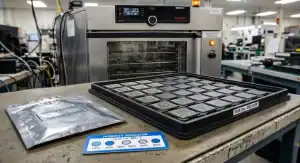
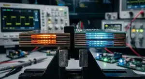
Table of Contents Buying electronic components is straightforward, but watching those expensive chips literally explode during assembly is a financial nightmare. You…
Engineering Change Notice (ECN) for PCB: How to Manage Design Changes Without Derailing Production
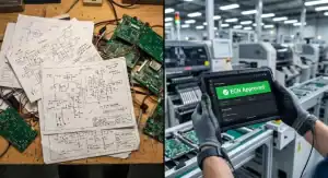
Table of Contents You realize mid-production that a component needs changing to avoid a shortage. You shoot a quick email to your…
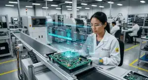
How to Audit a PCB Assembly Factory: The 8-Point Checklist Before You Sign a Contract
Table of Contents Many hardware teams skip the facility evaluation, relying entirely on a slick website and an aggressively cheap quote. This…
The Ultimate PCB Assembly RFQ Checklist For Engineers
Table of Contents You send out a request for quote and wait a full week, only to receive an estimate that feels…
How to Calculate True PCB Assembly Lead Time for Production
Table of Contents Missing tight project deadlines costs hardware startups thousands of dollars daily. You send your design files to a manufacturer,…
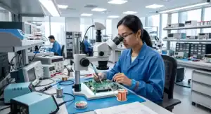
How to Use Solder Wick for Flawless PCB Rework Every Time
You face a dense circuit board, attempting to replace a faulty microchip, but your tools just smear the old metal across the…

How to Apply IPC Standards for PCB Assembly Success
You design a perfect board, send it to a manufacturer, and receive a batch that fails in the field because the factory…
How to Prevent Tombstoning SMT: 10 Proven Factory Fixes
Table of Contents To stop a component from standing on one end, you must perfectly balance the thermal mass and solder wetting…
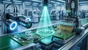
How to Decide Between AOI vs X-Ray vs ICT Testing
Table of Contents Hardware engineers often struggle to balance defect coverage with testing costs. You do not want field failures, but paying…

How to Fix BGA Voiding: Stencil Design & IPC Limits
Table of Contents Does your assembly partner claim your boards pass the bga voiding acceptable limits simply because they hit exactly 25%?…
4 Layer vs 6 Layer PCB: The Ultimate Cost & EMI Guide
Table of Contents Operating a facility with a 99.7% first-pass yield rate teaches you quickly where hardware teams lose money. Hardware engineers…
Top 10 PCBA Manufacturers in China [2026 Ranking for International Buyers]
Table of Contents Finding the right production partner in China is no longer just about the lowest price; it is about matching…