
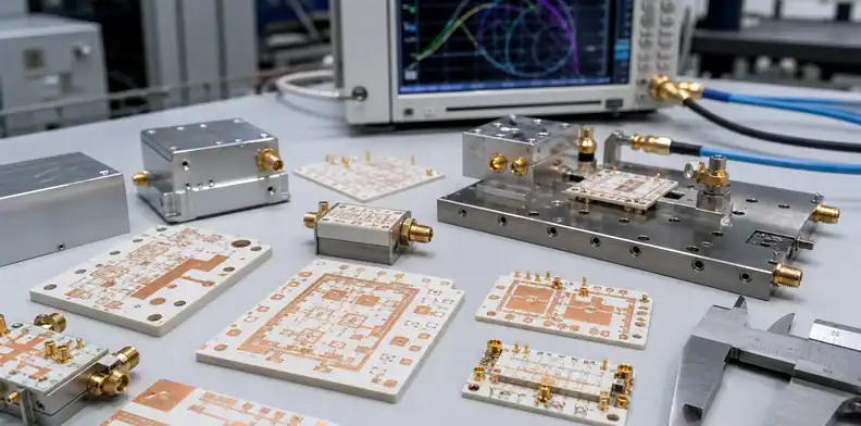
Quick Answer: Select a ceramic PCB for microwave and 5G mmWave modules by the operating band, dielectric loss, thermal load and package functions. Alumina, AlN, LTCC and thin-film ceramic serve different application needs; compare them with qualified low-loss laminate where appropriate. This page addresses material performance and module selection, with RF layout and DFM covered in the linked design article.
- RF and microwave ceramic decisions should start with frequency, loss budget, package size, and test method.
- LTCC, thin-film ceramic, alumina, AlN, and hybrid RF laminate solve different manufacturing problems.
- Overseas buyers should verify dielectric data, metallization route, tolerance, assembly boundary, and RF evidence.
The practical RF sourcing problem is not “ceramic is better.” A 2.4 GHz antenna module, 6 GHz front-end board, 24 GHz radar module, 28 GHz 5G mmWave package, and 77 GHz sensing product do not place the same demand on the substrate. Some designs belong on low-loss organic laminate; some need a ceramic package or LTCC structure; some need a small ceramic interposer or heat-spreading substrate inside a larger assembly.
For an RF, microwave or 5G mmWave module, compare substrate routes using dielectric data at the operating band, package geometry and the required test evidence. Once the route is selected, use the ceramic PCB RF layout rules and DFM guide to develop trace geometry and fabrication requirements.
Table of Contents
- What Does Ceramic PCB Change in Microwave and mmWave Modules?
- Which Ceramic Route Fits the Microwave or 5G Application?
- When is LTCC the right shortlist option?
- When should buyers stay with hybrid RF laminate instead?
- What RF data belongs in the ceramic PCB RFQ?
- How Do Assembly, Cavities and Shielding Affect Module Performance?
- What Evidence Qualifies the Chosen Microwave Substrate?
What Does Ceramic PCB Change in Microwave and mmWave Modules?
A ceramic PCB changes the RF module decision by tightening the relationship between dielectric behavior, package geometry, thermal path, and manufacturing tolerance. At RF and microwave frequencies, the substrate is not only a carrier for copper. It becomes part of the electrical model that controls impedance, insertion loss, resonance, phase, and coupling.
Ceramic materials can offer dimensional stability, high-temperature capability, useful thermal paths, and package-style construction that ordinary FR-4 cannot provide. Some ceramic systems also support integrated cavities, metallized vias, multilayer routing, or high-density package features. Those advantages matter when the design is small, high frequency, thermally dense, or close to a device package.
The risk is that “ceramic PCB” is a broad label. One supplier may mean alumina thick-film circuit. Another may mean AlN substrate with copper. Another may mean LTCC multilayer module. A fourth may mean thin-film ceramic for precise microwave lines. The RFQ has to identify the route, because the dielectric constant, loss tangent, conductor surface, via structure, and tolerance all change.
Start by naming the RF function: antenna feed, filter, coupler, power amplifier substrate, radar module, mmWave package, sensor board, or mixed RF/digital assembly. Then name the frequency band and the performance items that must be measured or preserved.
Use ceramic when RF performance, package density, heat, or tolerance requires it; do not choose it only because the product says 5G or microwave.
Which Ceramic Route Fits the Microwave or 5G Application?
The right ceramic route depends on whether the module needs a simple thermally stable circuit, a high-precision microwave path, or an integrated multilayer package. Alumina, AlN, LTCC, thin-film ceramic, and hybrid laminate all occupy different positions in the sourcing map.
Use three independent acceptance rows before comparing prices: RF performance across the specified band; the heat path at the stated load and cooling condition; and the required package functions. Record each as supported, incompatible, or not yet demonstrated. Missing data keeps a candidate open for investigation; it is not evidence of failure.
| Screen | Evidence that closes it | Decision if evidence is absent |
|---|---|---|
| RF | Comparable loss, match and phase data for the proposed structure and ports | Request a representative circuit measurement |
| Thermal | Device temperature or thermal model with attachment and cooling defined | Resolve the heat path before committing a substrate |
| Package | Drawing and process confirmation for cavities, feedthroughs, lid and attachment | Check a different package or split architecture |
Imagine an RF-module shortlist in which one candidate meets the straight-line loss target but cannot provide the required cavity, while another can form the cavity but has only unmeasured package transitions. This is an illustrative selection exercise. Neither quotation yet describes a demonstrated complete module, but the missing evidence points to different next steps.
For the first route, have the package designer show whether a separate cavity housing can preserve the required connections, dimensions and heat path. Price and assess that revised assembly, including the new interfaces. For the second, request a representative transition structure with the intended launch and return geometry, an agreed frequency range and defined measurement planes. A straight transmission-line sample does not close that transition question.
Return both responses to the same RF, thermal and package acceptance rows. Retain raw measurement files and the drawing revision associated with any sample; identify which package functions remain untested. A candidate that closes one gap may still leave another unresolved. The useful outcome is a specific next experiment or architecture change, rather than a material ranking based on whichever supplier supplied the most complete-looking datasheet.
The Ceramic PCB Guide sets the wider material map; RF selection also needs the operating band, loss target, conductor geometry, and packaging transition on the same RFQ.
Alumina is often reviewed for stable, cost-conscious ceramic RF circuits, especially when the board needs insulation, dimensional stability, and a familiar ceramic base. AlN enters the discussion when RF function is paired with heat, such as power amplifier, laser/RF mixed modules, or compact packages that cannot tolerate a weak thermal path.
Thin-film ceramic may be reviewed when precise conductor geometry and microwave performance are central. LTCC becomes relevant when the module needs multilayer ceramic integration, embedded passive structures, vias, cavities, or compact packaging. Hybrid RF laminate remains useful when the design is primarily PCB-like but needs low-loss material, controlled impedance, and a larger board format.
| Module need | Common shortlist | Buyer question |
|---|---|---|
| Stable RF circuit on ceramic | Alumina ceramic PCB | Is loss, tolerance, and finish acceptable at the band? |
| RF plus heat spreading | AlN ceramic substrate | Does the thermal path justify AlN cost and sourcing effort? |
| Integrated multilayer RF package | LTCC | Are vias, cavities, shrinkage, and supplier capability controlled? |
| High-precision microwave line | Thin-film ceramic | Can the supplier hold conductor geometry and finish? |
| Board-level RF routing | Hybrid low-loss laminate | Is ceramic truly needed or is RF laminate enough? |
Confirm the proposed ceramic and conductor combination with the ceramic manufacturing review. Include the RF package features that distinguish this build from a simple metallized carrier.
Select the supplier category after the RF structure is named; a laminate fabricator, ceramic substrate maker, and LTCC package supplier may not quote the same deliverable.
When is LTCC the right shortlist option?
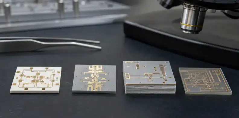
For an example of what the process can integrate, Orbray’s LTCC overview describes multilayer glass-ceramic structures, embedded RF passives and a supplier-specific process that constrains in-plane shrinkage. These are capabilities of the identified material system; they do not establish that every LTCC supplier can reproduce the same package.
LTCC can fit filters, antennas, front-end modules, sensor modules, compact packages, and RF structures where vertical interconnect, embedded passive behavior, cavity features, or small size matter. It may also help when the module must combine RF routing with mechanical package functions.
The buyer should not move to LTCC without recognizing the qualification load. LTCC has its own design rules, shrinkage compensation, via limits, conductor materials, firing process, cavity rules, and test expectations. A normal ceramic PCB supplier may not have LTCC capability, and a normal PCB assembly partner may not be able to repair a weak LTCC design after fabrication.
RFQ files for LTCC should include more than Gerbers. Send the stackup concept, layer functions, via plan, cavity or seal notes, frequency band, controlled impedance or resonator target, conductor material if specified, assembly interface, and test method. Ask the supplier to identify which dimensions are post-fired, which are controlled by process compensation, and which features need engineering review.
Choose LTCC when multilayer ceramic integration is the reason; if the need is only a low-loss trace on a board, review RF laminate or thin-film ceramic first.
When should buyers stay with hybrid RF laminate instead?
Buyers should stay with hybrid RF laminate when the design is board-level, the frequency and loss budget can be met with low-loss material, and the project needs ordinary PCB routing, larger formats, connectors, or mixed digital/RF assembly. Ceramic is not always the fastest or safest answer.
Many RF products use PTFE, hydrocarbon ceramic-filled, or other low-loss laminate systems rather than ceramic PCB. Rogers positions its high-frequency circuit materials around controlled dielectric properties and RF performance for antenna, radar, and communication applications. Those materials may fit a board-level RF product better than a ceramic route when the design needs familiar PCB fabrication and assembly.
The decision becomes sharper at mmWave. Higher frequency does not automatically require ceramic, but it reduces tolerance for material substitution, copper roughness surprises, via transitions, connector launch changes, and unmodeled dielectric behavior. If the design already has a qualified stackup on RF laminate, moving to ceramic may create more risk than it removes.
Use the QueenEMS article on Shengyi mmWave77 ceramic PTFE laminate when the real question is low-loss laminate selection. Use ceramic when the RF structure, package density, thermal path, or environmental need is truly ceramic-driven.
Stay with RF laminate when the product is a PCB stackup problem; move to ceramic when the module is also a package, heat, precision, or integration problem.
What RF data belongs in the ceramic PCB RFQ?
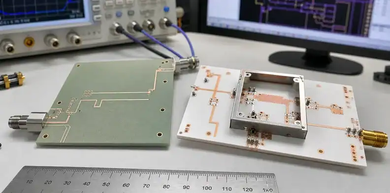
A ceramic RFQ should include the RF data that controls the electrical model: frequency band, impedance target, tolerance, line geometry, dielectric constant basis, loss tangent basis, copper or conductor thickness, surface finish, via structure, ground strategy, and test method. Without those fields, suppliers may quote different products under the same name.
Do not send only Gerbers and ask for “RF ceramic PCB.” Add the stackup, material target if known, dielectric values used in simulation, trace-width assumptions, reference-plane assumptions, via/cavity notes, finish, assembly temperature, connector or package interface, and the coupon structures and measurement deliverables to be supplied.
The buyer should also specify what may change. For early prototypes, the supplier may propose alumina, AlN, LTCC, thin-film, or hybrid laminate options if the design is still open. For production, material substitution should require engineering approval because a small dielectric change can move impedance, phase, filter response, or antenna tuning.
| RFQ field | Why it matters |
|---|---|
| Frequency band | Prevents generic dielectric claims from being used at the wrong range |
| Dk and Df basis | Keeps simulation values and supplier data aligned |
| Stackup and conductor route | Defines impedance, loss, manufacturability, and cost |
| Via/cavity/shielding notes | Determines whether PCB-like or package-like capability is needed |
| Test evidence | Connects the quote to coupon, S-parameter, impedance, or inspection records |
Before detailed routing, identify the RF port locations, package interfaces and tests that the quotation must include. Carry the approved route and stack revision into the layout review.
A useful ceramic RF supplier response states the material route, dielectric data basis, conductor process, tolerance limits, and test evidence before quoting production.
How Do Assembly, Cavities and Shielding Affect Module Performance?
Assembly, cavities, and shielding can decide whether a buyer needs a ceramic PCB fabricator, ceramic package specialist, LTCC house, or PCB/PCBA partner. RF performance often changes at the module boundary, not only in the flat trace section.
Package-style ceramic work may include cavities, lids, metallized walls, vias, ground fences, solderable pads, wire-bond areas, or die attach surfaces. Capability on a flat ceramic circuit does not establish cavity, seal or die-attach capability. A PCB assembler may mount components but may not control ceramic firing, metallized cavities, or RF package flatness.
Shielding and enclosure interfaces deserve early review. A metal lid, frame, absorber, connector launch, coax transition, or antenna radome can shift RF behavior if the mechanical stack is not controlled. The RFQ should show which parts are in scope and which will be added later by the buyer.
Assembly heat and cleaning also matter. Ceramic substrates may tolerate heat, but the metallization, finish, components, adhesives, and package seals still have process limits. Ask whether the quote covers bare substrate, mounted components, die attach, wire bonding, lid attach, cleaning, inspection, or only a ceramic circuit panel.
Define the deliverable as bare substrate, ceramic package, assembled RF module, or controlled handoff; the supplier choice changes with that boundary.
What Evidence Qualifies the Chosen Microwave Substrate?
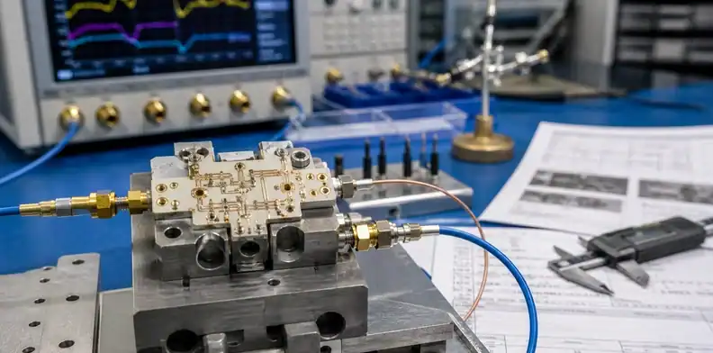
Qualify the proposed microwave substrate using the actual material family, conductor process, package features and measurements across the operating band. Request the dielectric data basis, tolerances, surface finish, via or cavity construction and relevant RF test evidence for the selected route. A general RF capability statement does not close those application-specific questions.
A strong first response asks technical questions. It will ask about frequency band, stackup, impedance, dielectric assumptions, package interface, thermal load, assembly scope, test method, and whether the project is prototype or production. A weak response quotes from keywords and never asks what frequency or measurement matters.
For prototypes, speed and DFM clarity matter. The buyer may need the supplier to say which shortlisted construction is ready for fabrication. For production, documentation matters more: controlled drawings, material records, process route, inspection data, packaging labels, change-control rules, and RF evidence.
QueenEMS fits projects where the overseas team needs RFQ coordination, ceramic route screening, PCB/PCBA handoff, English engineering communication, and documentation. The role is not to replace a specialized LTCC or ceramic package house when that exact capability is required; it is to help buyers define the quote path and keep prototype or low-volume builds controlled.
Approve a ceramic RF supplier only after the quote ties the substrate route to the frequency band, tolerance, assembly scope, and evidence request.
FAQ
Is ceramic PCB always best for 5G mmWave?
No. Some mmWave designs need ceramic package or LTCC capability, while others work better on qualified low-loss RF laminate. The right answer depends on frequency, loss budget, package size, thermal path, tolerance, and test method.
What is the difference between LTCC and ceramic PCB?
LTCC is a multilayer co-fired ceramic technology used for compact integrated structures. Ceramic PCB is a broader term that may include alumina, AlN, thick-film, thin-film, DPC, DBC, or other ceramic circuit routes.
What should I send for an RF ceramic PCB quote?
Send Gerber or ODB++ files, stackup, frequency band, impedance requirements and the model’s dielectric assumptions, conductor and finish requirements, via/cavity notes, assembly scope, test requirement, quantity, and controlled-substitution rules.
Can QueenEMS quote RF ceramic PCB prototypes?
QueenEMS can help review the RFQ path for ceramic PCB prototypes and low-volume builds, including material route, DFM questions, fabrication scope, and assembly coordination when appropriate. Specialized LTCC or ceramic package work may require a process-specific supplier route.
Which Dielectric Data Matter for a 5G mmWave Module?
Compare dielectric constant and loss using the relevant frequency and measurement method, then evaluate the proposed conductor, transitions and package in the module model. A low-frequency material value alone does not qualify a 5G mmWave application.
Send QueenEMS an RF ceramic PCB module RFQ
For an RF-module quotation, submit the port definition, operating band, stack proposal and required package functions through the project inquiry form. Attach the circuit files, thermal boundary conditions, assembly scope and acceptance plan so unresolved route choices can be identified before pricing.
Sources
- Orbray: LTCC materials and processing
- Rogers Corporation, High Frequency Circuit Materials
Written by the QueenEMS Engineering Team
Upload your files today · Free DFM check before production · Ship worldwide
Get your PCB prototypes in as fast as 24 hours. We handle FR4, Rogers, and Flex up to 60 layers — free prototypes for 2–4 layer boards, no minimum order.
Just upload your Gerber + BOM — we source every part, assemble, and inspect (AOI + X‑Ray) so you don't have to chase suppliers. Boards ship in as fast as 24 hours.