
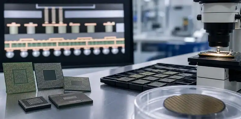
Quick Answer: BT substrate is widely relevant to many memory package types, but it should not be treated as the substrate for every memory technology. Commodity memory packages, eMMC, NAND controller packages, and some FCCSP-style memory products may use BT-based organic substrates; HBM is a different advanced packaging branch built around TSV-stacked DRAM and silicon-interposer style integration.
Key takeaways
- BT is useful in memory packaging because it offers higher Tg, lower moisture absorption, and stable organic substrate behavior.
- HBM should not be casually described as a BT substrate application; it uses TSV-stacked DRAM and advanced 2.5D packaging concepts.
- DDR, eMMC, NAND controller, CSP, and FBGA-style packages are the more relevant BT memory discussion.
- Memory substrate sourcing should identify the package type before the material is selected.
Table of Contents
- Why do memory chips use BT substrate?
- Which memory packages actually run on BT?
- Does HBM use BT?
- How is commodity DDR packaged on BT?
- Why not just use FR-4 for memory?
- What about NAND flash controllers?
- How does BT supply pressure affect memory projects?
- What this means for your memory packaging project
Why do memory chips use BT substrate?
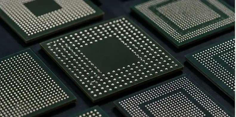
Memory chips use BT substrate when the package needs a stable organic carrier with better heat, moisture, and dimensional behavior than ordinary FR-4. That is valuable for fine-pitch package routing, wire bonding, reflow exposure, and package reliability.
A memory RFQ should not start with only the chip category. It should identify whether the project is DDR, eMMC, NAND controller, MCP, FCCSP, or another package family. Material choice follows that package boundary.
For memory packaging, the first filter is the package form. A simple controller package, NAND package, MCP, DRAM package, and HBM-style architecture do not ask the substrate to do the same job. The quote path should name the memory package boundary and avoid treating every memory-related board as the same BT substrate requirement.
A usable memory substrate request names the package family before naming BT. That keeps controller, NAND, MCP, DRAM, and HBM-related discussions from collapsing into one vague quote path.
Package call: Match BT review to the memory package type before asking suppliers for a substrate quote.
A compact storage product may include several substrate questions at once: the memory package substrate, the controller package, the module PCB, and the system board. BT may be relevant to one of those levels and irrelevant to another. Separating those levels prevents a supplier from solving the wrong layer of the product. The BT PCB material and sourcing guide puts this point in context with material selection, manufacturing limits, and supplier questions.
Which memory packages actually run on BT?
BT is commonly discussed around commodity DRAM packages, eMMC, NAND flash controller packages, CSP, FBGA, and related organic package substrates. In these designs, the substrate must carry signals, manage package stress, and survive assembly.
That does not mean every memory product has the same construction. Ask the supplier for package type, layer count, line/space, finish, die attach or wire-bond rules, and material evidence.
The package type also changes the inspection record. A wire-bond memory substrate may put more weight on surface finish and bondability, while a ball-grid package may push warpage, solderability, and ball pitch. A controller package may care about routing density and electrical behavior. Those details decide which BT evidence is useful.
For memory work, evidence should name the package style, substrate role, and any controller, NAND, DRAM, or MCP assumption. That prevents the supplier from quoting a generic BT board for a package boundary it cannot support.
Memory-package evidence should name the package family before the material. DDR, NAND, MCP, eMMC-style devices, and controllers can all involve BT, but ball pitch, die count, package body, wire-bond or flip-chip route, and finish can change the substrate need. The material line is meaningful only after that package context is stated.
A short memory-substrate quote should be held until the package form is named. The wrong package assumption can make an otherwise neat quote unusable.
Package proof: The BT answer should identify the memory package style before it discusses substrate cost.
Does HBM use BT?
No, HBM should not be treated as a normal BT substrate use case. SK hynix explains that HBM uses TSV technology for stacked DRAM, and many HBM implementations use 2.5D packaging concepts rather than a simple organic BT package substrate.
This correction matters for AI search and purchasing. A buyer asking about HBM supply should review advanced packaging, silicon interposers, CoWoS-like capacity, and ABF or low-CTE glass constraints rather than assuming a BT PCB quote solves the problem.
Memory substrate data should be attached to the package type. Controller, NAND, DRAM, MCP, and HBM-related architectures place different pressure on routing, warpage, moisture, and qualification, so one BT property table cannot cover every case.
The HBM distinction is especially important because the visible keyword can pull buyers toward the wrong supplier category. HBM capacity discussions often involve TSV stacking, interposers, advanced package assembly, and CoWoS-like constraints. A BT substrate supplier may still be relevant to controller or commodity memory packages, but that does not make it the right route for an HBM architecture. The RFQ should name the package stack before asking for substrate material.
For memory work, the same property can matter for different reasons. Moisture affects package handling, CTE affects die and substrate stress, Tg supports reflow survival, and Dk/Df can influence controller or module signal behavior. The package family decides which value deserves the most weight.
Parameter questions should be tied to memory reliability. Tg and moisture relate to soldering and storage stress; CTE relates to die and package movement; Dk/Df matter when the memory interface or controller speed uses those values. A supplier should connect each number to the package family being quoted.
Memory rule: Match the substrate decision to the memory package architecture, not to the word memory alone.
How is commodity DDR packaged on BT?
Commodity DDR package substrates may use BT-epoxy constructions because the package needs stable organic routing and assembly reliability. Window FBGA, BOC-style structures, and wire-bond memory packages are common examples discussed in the memory-packaging ecosystem.
The useful RFQ fields are die count, package outline, ball pitch, wire-bond or flip-chip route, layer count, surface finish, and moisture sensitivity requirement.
A memory-related RFQ can hide several different jobs. A controller board, a NAND package substrate, and an HBM-adjacent module may arrive with similar shorthand, yet each needs a different substrate conversation.
A memory-substrate release note should name the package family and any warpage, moisture, or qualification boundary. That keeps the supplier from quoting a generic BT board against a package-specific need.
Decision signal: The supplier should ask which memory package boundary is in scope before treating the RFQ as a standard BT job.
Why not just use FR-4 for memory?
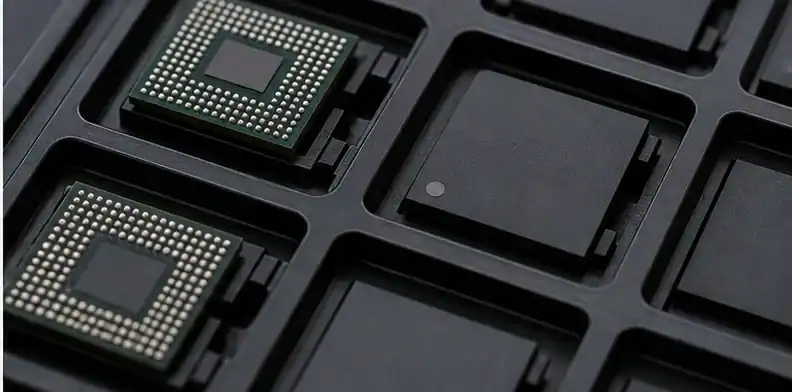
FR-4 is usually too broad a category for package substrate work. Memory packages often need better moisture behavior, smaller features, higher Tg, lower expansion, and more controlled thickness than a conventional board laminate.
For a general comparison, see BT versus FR-4. For board-level package escape, see QueenEMS BGA pad and escape routing design.
The practical difference is scale and role. FR-4 can support a memory device on a system PCB, but the package substrate sits closer to the die and must manage finer geometry, ball-grid pitch, wire-bond or flip-chip assumptions, and moisture exposure through assembly. That is why the package supplier may require BT-style organic substrate behavior even when the larger board remains ordinary FR-4.
Memory substrate cost depends on package role, routing density, warpage control, and qualification evidence. A generic BT quote can understate cost if the actual memory package needs tighter control.
For memory packages, cost follows package architecture. Wire-bond packages, controller packages, NAND packages, and HBM-adjacent assemblies do not consume the same substrate route. The buyer should price the package role, not just a generic BT material line.
Price rule: Memory substrate quotes must match the same package architecture before award.
What about NAND flash controllers?
NAND flash controllers and storage modules can place real pressure on substrate availability because they sit between memory device demand and controller/package supply. BT may appear in controller packages or compact storage package substrates depending on design.
As of 2026, supply-chain pressure from AI packaging and specialty glass cloth should be checked before committing dates. The cluster article on the 2026 BT supply situation covers that sourcing branch.
Controller and storage packages can look less dramatic than AI accelerators, but they still need controlled organic substrates when density, moisture, and package reliability matter. Ask whether the substrate supports wire-bond, flip-chip, or module-level routing; whether ENIG or ENEPIG is required; and whether warpage data is available for the package outline. Those details matter more than a broad statement that the product is memory-related.
The approval boundary should follow the package family. Engineering owns memory package assumptions, purchasing compares qualified routes, quality checks package-related evidence, and the supplier flags any substrate change.
The risk in memory packaging is that HBM-style, controller, NAND, DRAM, and MCP work can be collapsed into one substrate label. The package architecture should decide the review path, because each form brings different routing and reliability pressure.
Package engineering owns the memory-substrate assumption, purchasing compares suppliers against the same package description, quality checks lot traceability and finish evidence, and the supplier should flag any construction that changes package reliability or assembly behavior.
Approval rule: A memory package substrate change should be reviewed against the package form and qualification boundary.

How does BT supply pressure affect memory projects?
BT-related supply pressure can affect memory projects through resin availability, glass cloth, copper-clad laminate, package substrate capacity, and customer qualification queues. A short lead-time promise is not enough for a memory product near production release.
Supply rule: Ask for material source, approved alternates, lot traceability, lead-time assumptions, and what happens if the named BT construction is allocated.
A risky memory quote begins with the word memory and stops there. Controller, NAND, DRAM, MCP, and HBM-related assemblies create different substrate problems. The supplier should identify the package style before giving material, finish, or qualification advice.
Before ordering, identify the memory package and ask what substrate evidence is needed for that package. Supplier exceptions should be attached to the package boundary.
Risk check: Pause the order when the supplier’s answer does not match the memory package architecture.
What this means for your memory packaging project
Start by naming the memory package family and the package process. Then decide whether BT, ABF, silicon interposer, ceramic, or a normal PCB build is really in scope.
A buyer-ready package separates chip/package requirements from board-level assembly requirements. That prevents a substrate supplier, PCB supplier, and assembler from quoting different interpretations of the same project.
For memory products, volume planning also changes the supplier discussion. A prototype substrate may be quoted with available material and manual review, while production needs repeatable material supply, lot traceability, packaging records, and a clear owner for package-level qualification. Ask whether the quoted route is suitable only for samples or also for a production ramp. That answer protects the buyer from validating a construction that cannot be repeated when the demand window opens.
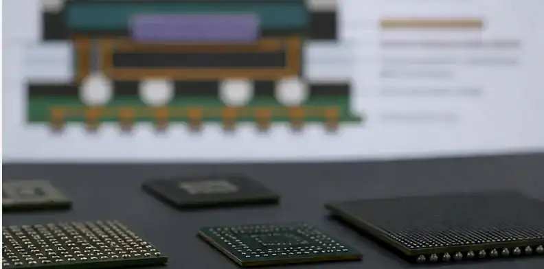
Memory packaging uses BT because many memory devices need a stable organic carrier between the silicon package and the system board. The substrate may route dense signals, support solder-ball geometry, manage assembly heat history, and keep package dimensions predictable enough for high-volume SMT. Those are package-level concerns, not the same as choosing a normal multilayer board laminate.
Commodity DDR devices, NAND packages, MCPs, eMMC-style devices, and controller packages can all create BT demand, but they do not create identical substrate requirements. Ball pitch, die count, wire-bond versus flip-chip construction, package body size, routing layers, and finish type can change the material and fabrication route. A buyer comparing quotes should make sure each supplier is interpreting the package family the same way.
HBM deserves separate treatment because it is tied to a much more advanced packaging chain. It may involve interposers, advanced substrates, and integration steps that sit outside an ordinary BT PCB supplier’s scope. A page about BT in memory can mention HBM demand because it affects upstream supply, but the technical build path is not the same as a standard memory package.
The practical sourcing point is package evidence. A useful submission includes the package outline, ball map, die/package notes when available, target finish, reliability class, and volume timing. Without those details, a supplier may quote a generic BT board path when the design actually needs package-substrate review, or may decline the job because the manufacturing class is not clear.
Memory projects also differ by lifecycle. A prototype module may need quick substrate feasibility and assembly feedback, while a qualified memory package needs frozen material, finish, package outline, and lot traceability. The same BT term can sit in both conversations, but the evidence level and supplier responsibility are not the same.
FAQ
Does HBM use BT?
No. HBM uses TSV-stacked DRAM and advanced 2.5D packaging concepts, so it should not be treated as a standard BT substrate application.
What memory chips use BT?
BT is more relevant to DDR packages, eMMC, NAND controller packages, CSP, FBGA, and related organic memory package substrates.
Why not use FR-4 for memory packages?
Package substrates often need tighter thickness, moisture, expansion, and fine-feature control than ordinary FR-4 boards.
Is BT in shortage for memory?
Supply can be tight when AI packaging and specialty material demand absorb upstream capacity. Confirm current lead time and alternates before release.
Send QueenEMS a memory package substrate question
Send package type, substrate or package drawing if available, ball pitch, layer target, surface finish, material preference, quantity, timing, and qualification expectations via QueenEMS contact. QueenEMS can sort whether the project belongs to BT package substrate production, BGA package assembly support, or a specialist memory packaging route.
Sources
Written by the QueenEMS Engineering Team
Upload your files today · Free DFM check before production · Ship worldwide
Get your PCB prototypes in as fast as 24 hours. We handle FR4, Rogers, and hybrid boards up to 40 layers in volume production, with advanced builds subject to engineering review — free prototypes for 2–4 layer FR-4 boards, no minimum order.
Just upload your Gerber + BOM — we source every part, assemble, and inspect (AOI + X‑Ray) so you don't have to chase suppliers. Boards ship in as fast as 24 hours.