
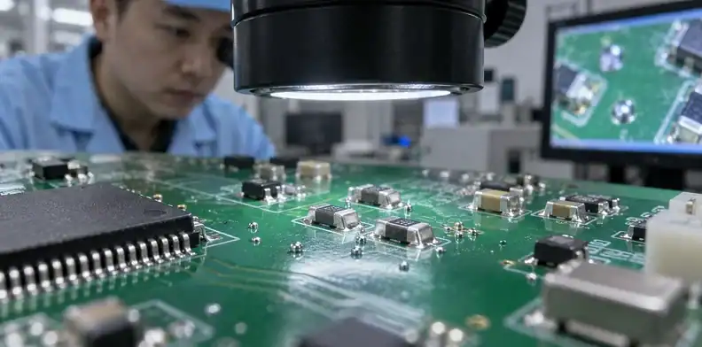
Quick Answer: Prevent unwanted solder balls by first identifying their pattern, then checking the paste, printing, placement and measured thermal conditions associated with that pattern. Random spattering and beads beside chip components can have different mechanisms, so one oven adjustment is not a universal cure. Contain affected assemblies, retain evidence before removal and confirm the correction without creating inadequate solder joints.
Solder balls found after reflow are evidence of a process problem to investigate, not an instruction to turn the oven up or down. The first useful distinction is between intended package spheres and unintended particles; the next is between scattered balls and repeatable beads near specific components.
This article focuses on unwanted solder particles in PCB assembly. It does not cover buying spheres for BGA reballing. Use the investigation sequence below to preserve the failure pattern, narrow the cause and judge whether a proposed correction has enough evidence to support production release.
Table of Contents
- Identify loose solder balls, beads and intended BGA spheres
- Contain affected assemblies before cleaning them
- Use the particle location to narrow the investigation
- Check solder paste handling and moisture exposure
- Look for paste outside the intended deposits
- Treat chip-component beading as a separate branch
- Measure the board profile before changing oven settings
- Separate wave-solder particles from reflow defects
- Verify the correction beyond the first clean-looking board
- Request a corrective-action package that can be tested
Identify loose solder balls, beads and intended BGA spheres
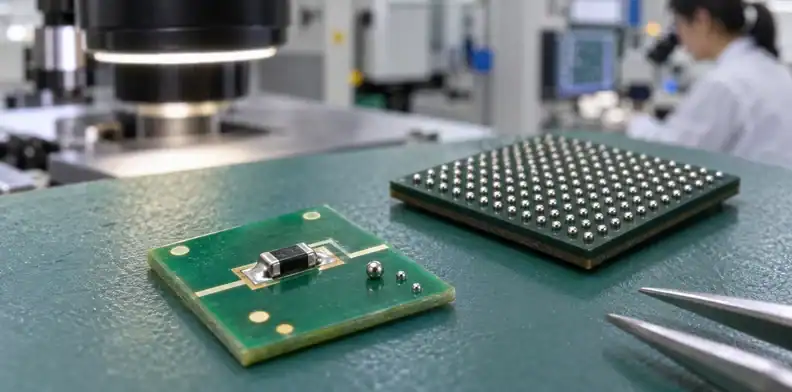
Identify the object’s role and location before calling it a defect. Balls designed into a ball-grid-array package are electrical interconnects; loose particles on solder mask are a different issue.
| Appearance or location | Likely category | What must be established |
|---|---|---|
| Ordered sphere array beneath an unassembled package | Intended BGA spheres | Package identity and intended attachment process |
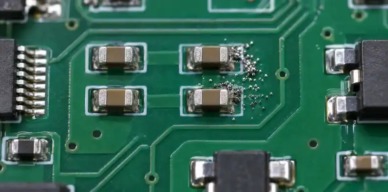
| Small random satellites around joints or across mask | Balling or spattering | Where and when particles first appeared |
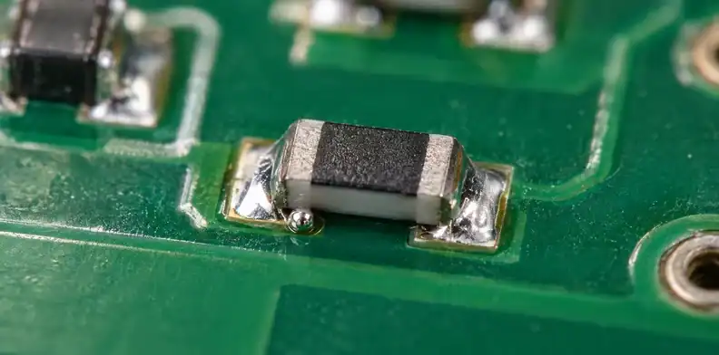
| Larger bead beside a chip resistor or capacitor | Localized solder beading | Deposit, component gap and placement relationship |
| Continuous connection between conductors | Solder bridge | Actual electrical connection and joint geometry |
AIM’s SMT troubleshooting material distinguishes random balling from localized beading. The terms describe useful investigation branches, not a substitute for microscopy or the product’s acceptance requirements. Photograph the affected area with scale and reference coordinates.
Do not assume every bright dot is solder. Reflections, exposed finish and other debris can resemble metallic spheres in a low-resolution image. Confirm the material and physical condition using an appropriate inspection method before planning removal.
The intended package-joint route belongs to BGA component assembly, not to a stray-particle repair instruction. A bridge, an inadequately wetted joint and a loose ball can coexist, but solving one does not establish that the others are absent.
Contain affected assemblies before cleaning them
Hold the affected population and preserve the original evidence before removing particles. Cleaning first can erase the pattern needed to locate the process failure and determine how far it extends.
Record the board identity, lot, side, component reference and process stage. Take an overview and magnified images of representative particles. Identify whether the condition occurs on one board, throughout a panel or across builds made with the same paste or setup.
The immediate risk depends on the particle’s location, mobility and product environment. A conductive particle can cause a short if it reaches adjacent conductors; a functional test performed while it remains elsewhere does not demonstrate that it cannot move later. Keep containment separate from the final acceptability decision.
Use the agreed product drawing, contract and applicable acceptance standard, including its revision and class. Do not substitute an internet diameter or count limit for the controlling requirement. Likewise, coating over a particle is not automatic authorization to retain it.
The lot identification and containment records help define which other units may share the condition. If the affected range is uncertain, preserve that uncertainty rather than recording an unsupported narrow boundary.
Removal must follow an approved method that protects components, finishes and electrostatic-sensitive devices. Avoid improvised air blasting that merely transfers particles to hidden areas. After removal, inspect relevant crevices and perform the required checks; a cleaner photograph alone is not a complete lot-release record.

Use the particle location to narrow the investigation
Map where particles occur and compare that map with the printing and placement sequence. Location can suggest a hypothesis, but it does not prove the cause by itself.
| Recurring pattern | Hypothesis to examine | Discriminating evidence |
|---|---|---|
| Near one stencil opening on many boards | Local print or aperture problem | Before-placement images and deposit data |
| Beside the same passive component | Paste displaced beneath the body | Print versus post-placement comparison |
| Random satellites across multiple areas | Paste condition or volatilization issue | Handling history and measured thermal route |
| Appears only after wave soldering | Wave, flux or mask interaction | Inspection before and after that operation |
| Concentrated around one repair location | Rework-generated particles | Repair materials, method and surrounding inspection |
Examine the board at the earliest available stage. A picture after reflow cannot tell you whether paste was already smeared outside pads or moved there during placement. If the original build lacks those images, capture them in the next controlled trial instead of filling the gap with certainty.
An SPI pass does not exclude every stray deposit. A pad-centered region may miss material elsewhere on the mask, and paste can move after inspection. Request raw images or targeted visual checks alongside the numerical results.
Keep particle size, distribution and affected reference designators together. A change from widely scattered satellites to one repeatable mid-chip bead may mean there are two mechanisms, not a partial cure of one. Build separate hypotheses when the evidence warrants them, then choose the next test for its ability to distinguish those hypotheses.
Check solder paste handling and moisture exposure
Review the exact paste’s storage and use history against its current technical instructions. A fresh date code does not establish that the container was conditioned, opened and used correctly.
Inspect the container and floor-use history
Check the material identity, lot, storage record, opening time, conditioning procedure and elapsed use. Investigate whether worked paste was returned from the stencil and mixed with unused material; Kester advises against that practice. Those details can be more revealing than the operator’s recollection that the paste was “new.”
Kester’s handling guidance recommends natural equilibration to room temperature without forced heating. It also warns about condensation when opened containers are refrigerated. Use the actual formulation’s instructions for times and conditions; do not impose one warm-up or storage value on every paste.
Avoid adding unapproved solvents or flux to recover material that has changed consistency. Such an intervention changes the formulation and introduces another variable into the investigation. Hold questionable material for supplier-supported evaluation.
Separate moisture from poor coalescence
Moisture-related spattering and poor coalescence can produce superficially similar satellite particles. Oxidation, material condition and the thermal route may also be involved. The observation of balls alone does not identify which factor dominates.
A material comparison can help, provided the board, stencil and measured profile remain comparable. Keep a suspect-paste sample and the handling record rather than replacing the jar and declaring the cause proven.
Joint wetting is a related but separate question. Consult the cold solder joint diagnosis if assembled joints also show poor wetting, while keeping stray-particle formation as its own investigation.

Look for paste outside the intended deposits
Inspect both the intended pad deposits and unwanted paste around them. A print with acceptable pad volume can still carry smeared material that becomes balls after heating.
Inspect stencil underside and board contact
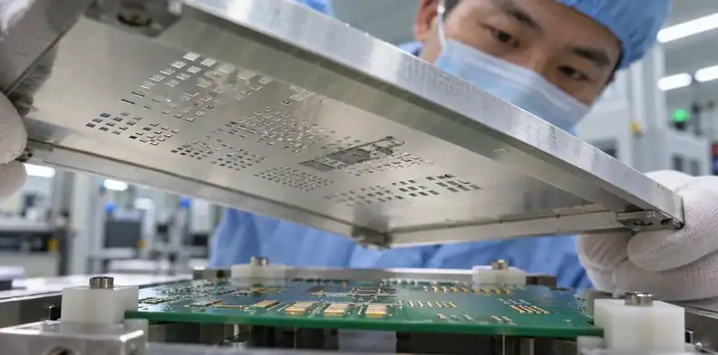
Look for underside contamination, poor gasket contact, board movement and localized support problems. Compare affected coordinates with the stencil cleaning sequence and earlier prints. Retain images before wiping the stencil so the proposed explanation can be checked.
If paste is already present between or outside pads, an oven adjustment is not the first correction to test. Review the printing condition that put it there. Changes to cleaning frequency or support should be evaluated on the next print as well as on the finished board.
Review aperture geometry with deposit evidence
Indium’s StencilCoach discussion describes tailored aperture concepts for passive components, including homeplate-related shapes. The relevant geometry depends on the component, stencil thickness and transfer behavior; it does not justify a universal paste-volume reduction.
Bring the released SMT stencil specification into that review. Confirm whether the problematic print matches the intended openings before redesigning them. A manufacturing defect in the stencil and an unsuitable aperture design call for different actions.
When reducing a deposit, check joint sufficiency in the same trial. Eliminating a bead by starving the joint merely exchanges defects. Compare the actual delivered paste, the subsequent joint and bead occurrence together, with enough repeated prints to reveal whether transfer remains stable.
Treat chip-component beading as a separate branch
A repeatable bead beside a chip component deserves a placement-and-deposit investigation distinct from random spattering. Paste beneath the body can be displaced as the component and solder settle during reflow.
| Evidence at the passive component | Question it raises | Controlled comparison |
|---|---|---|
| Paste migrates inward after placement | Is placement moving material under the body? | Before/after-placement images with unchanged print |
| Bead recurs at the same inside edge | Does aperture geometry encourage inward paste? | Tailored opening versus baseline |
| Different component lots behave differently | Do dimensions or standoff change the gap? | Actual component data and measured geometry |
| Fewer beads but inadequate joints | Was too much solder removed? | Joint inspection alongside particle count |
Ersa describes capillary movement and subsequent squeeze-out as a possible reflow mechanism. Use that mechanism to guide observation, not to claim that every bead has the same cause. Placement settings and component tolerances should be checked against the actual package and process.
An illustrative investigation starts with a bead beside one resistor even though its pad volumes pass SPI. Images show paste moving inward after placement. A trial changes only the relevant aperture approach while retaining the material and thermal route, then examines both bead recurrence and joint adequacy. This is a hypothetical engineering example, not a recorded QueenEMS result.
The component remaining flat does not eliminate beading. Conversely, a lifted end belongs to the tombstoning troubleshooting process.
Measure the board profile before changing oven settings
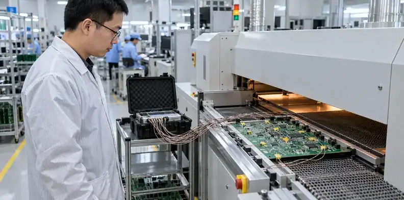
Measure temperatures on the affected assembly and compare them with the paste and component requirements. The oven recipe alone does not establish the thermal history at the deposit that produced the particles.
Capture temperatures at the affected locations
Use a suitable profiling setup with sensors attached to representative joints or locations, including thermally different areas. Record the actual heating rate, dwell, peak and cooling behavior relevant to the selected alloy and materials.
Do not borrow a published example’s numerical ramp or soak as a universal recipe. Board mass, component limits, paste chemistry and conveyor conditions affect the usable window. A correction must remain within all applicable material and component constraints.
Change one supported parameter at a time
AIM’s troubleshooting material shows why “slower is safer” is an incomplete rule: excessive or unsuitable heating can contribute to spattering, while slow heating can also contribute to some beading conditions. First identify the pattern, then use the current paste instructions and measured curve to choose a bounded change.
Keep the print and placement conditions fixed when testing a thermal hypothesis. If paste, stencil and oven settings all change at once, a cleaner board does not identify which adjustment mattered. Check the affected region and other thermally sensitive joints for unintended effects.
The wider SMT production route should preserve the approved profile and change history. Once a trial supports a revised setting, repeat the measured check under representative loading rather than assuming a favorable bench result transfers unchanged to production.
Separate wave-solder particles from reflow defects
Locate the operation that generated the particles before changing the process. A board may undergo reflow, wave or selective soldering and repair; material found at final inspection could originate at any of them.
| Route | Mechanisms worth checking | Evidence before adjustment |
|---|---|---|
| Paste reflow | Stray paste, coalescence, volatilization, local beading | Printed and placed board images; measured profile |
| Wave soldering | Separation, spitting, flux behavior, mask interaction | Before/after-wave inspection and process conditions |
| Selective soldering | Local flux and solder interaction near the processed area | Position-specific observations and machine route |
| Manual repair | Excess material or splatter around the reworked joint | Repair log, surrounding images and method |
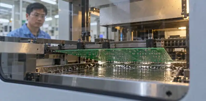
Ersa’s solder-ball discussion explains that wave separation and solder-mask behavior differ from reflow mechanisms. A stencil change cannot correct particles introduced only after a wave operation. Conversely, altering wave settings will not address paste already smeared during printing.
Inspect intermediate samples where the route allows it. Seeing the particles first after wave soldering is stronger evidence than assuming that all balls on an SMT-containing board arose in reflow. Preserve process-stage identity in the photographs.
The cleaning route is another independent variable. PCB cleanliness requirements concern residues and agreed tests; removing visible metallic particles does not establish ionic cleanliness, and passing a residue test does not prove that no movable metal remains.
Verify the correction beyond the first clean-looking board
Compare the correction with a documented baseline using the same inspection opportunity. One clean board is encouraging, but it does not demonstrate control of an intermittent defect.
| Trial record | Detail to preserve | Why it matters |
|---|---|---|
| Baseline | Units, inspected areas and particle observations | Establishes what changed |
| Controlled adjustment | One changed parameter and unchanged conditions | Supports a causal interpretation |
| Repeated trial | Representative boards and defined inspection method | Exposes intermittent recurrence |
| Joint quality | Relevant visual, hidden-joint or electrical checks | Detects defects exchanged for fewer particles |
| Continued production check | Approved recipe and follow-up observations | Tests whether the correction persists |
Kester’s historical engineering note, “10 Solder Tips,” describes a coalescence screen on a nonwetting surface to examine whether a paste deposit forms a central mass or leaves satellites. It can inform a supplier-supported material investigation. It is not a complete board-process qualification or a current customer acceptance test by itself.
Apply that distinction to a material trial: better coalescence with a comparison sample suggests a material-related path, but does not prove which storage event caused the original failure. Keep the handling evidence alongside the screening observation.
For an aperture trial, retain the former and revised geometry and examine solder sufficiency, not only the bead count. For a profile trial, preserve both measured curves. When findings conflict, hold the conclusion open; a corrective-action report is stronger when it states the unresolved question than when it assigns a convenient but untested root cause.
Request a corrective-action package that can be tested
Ask for evidence that links the observed particles to a specific cause hypothesis, controlled change and release decision. “Cleaned and reflow optimized” does not show why the next lot should behave differently.
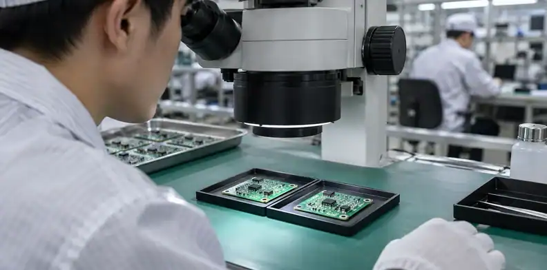
For an existing issue, provide scale photographs, affected references, build identity and the first stage at which particles were observed. Add the paste identity and handling history, stencil revision, print and placement evidence, actual thermal profile and any earlier removal or repair.
The supplier’s response should distinguish containment, correction of affected boards and prevention of recurrence. Those are separate outcomes. Confirm the inspected population, approved removal method, post-removal checks and the authority responsible for lot disposition.
For a new assembly quotation, identify known problem packages or prior failures and the evidence you expect from qualification. The assembler can then price the relevant trials instead of assuming that routine end-of-line inspection will answer a process-development question.
If you want a build proposal, send QueenEMS the solder-particle investigation package with the assembly files and affected-area evidence. It supports a scoped review of printing, placement, thermal trials and inspection work. Release still depends on the agreed product criteria and the results actually obtained, not a promise of zero particles from a generic process change.

Sources
- AIM Solder: SMT troubleshooting, including balling and beading.
- Kester: historical coalescence-screening example in 10 Solder Tips.
Written by the QueenEMS Engineering Team
Upload your files today · Free DFM check before production · Ship worldwide
Get your PCB prototypes in as fast as 24 hours. We handle FR4, Rogers, and hybrid boards up to 40 layers in volume production, with advanced builds subject to engineering review — free prototypes for 2–4 layer FR-4 boards, no minimum order.
Just upload your Gerber + BOM — we source every part, assemble, and inspect (AOI + X‑Ray) so you don't have to chase suppliers. Boards ship in as fast as 24 hours.