

Quick answer: A cold solder joint is an unreliable connection caused by incomplete wetting or an unsuitable soldering process. Look for shape, wetting, cracks, movement, or intermittent behavior—not color alone. Confirm the finding with magnified inspection and an appropriate electrical or functional test before reworking the joint.
A matte surface can be normal with some lead-free alloys. The assembly drawing, solder alloy, component termination, and applicable acceptance criteria determine whether a joint is acceptable.
A cold solder joint can pass a quick power-on check and fail later under vibration, temperature change, or mechanical load. The fastest route to a reliable fix is to separate three questions: Is the joint actually defective? What process condition caused it? How will the repair and the next build be verified?
Cold Solder Joint vs. Good Solder Joint: What Is the Difference?
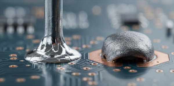
A sound joint shows acceptable wetting between the solder, pad, and component termination and has the geometry required for that connection. A cold or poorly wetted joint may have an irregular fillet, an exposed interface, a crack or ring around the lead, solder that beads away from the pad, or movement between the lead and solder.

| Check | Potentially acceptable | Needs investigation |
|---|---|---|
| Surface | Shiny or matte, depending on alloy and process | Grainy, disturbed, cracked, or contaminated appearance |
| Wetting | Solder transitions continuously onto the pad and termination | Non-wetting, dewetting, beading, or an exposed interface |
| Mechanical condition | Lead and joint remain stable under permitted handling | Movement, lifted pad, fractured fillet, or loose termination |
| Electrical behavior | Stable result under the intended test | Intermittent continuity, abnormal resistance, or functional failure |
Do not reject a joint only because it looks dull. Many lead-free finishes are less reflective than traditional tin-lead joints. Inspect the complete fillet and compare it with the product class, drawing, alloy supplier guidance, and the acceptance criteria used for the build.
How to Identify a Cold Solder Joint
Start with a visual check under suitable lighting and magnification. Examine the pad-to-solder and lead-to-solder interfaces from more than one angle. Look for incomplete wetting, disturbed solder, cracks, void-like surface openings, solder balls, bridging, lifted pads, or a lead that moves when it should be fixed.
- Compare suspect joints with known-good joints built with the same alloy and process.
- Review polarity, package alignment, pad condition, and component seating before blaming the solder joint.
- Use AOI or X-ray only where the package and defect type make those methods suitable.
- Record the location and symptom so the repair can be traced back to the process step.
For hidden or ambiguous faults, inspection alone may not be enough. Continuity, resistance, in-circuit test, boundary scan, or functional test can help, but the correct method depends on the circuit. A generic resistance cutoff is not reliable across power paths, signal nets, connectors, and parallel components. See how AOI, X-ray, and ICT answer different inspection questions.
What Causes Cold or Poorly Wetted Solder Joints?
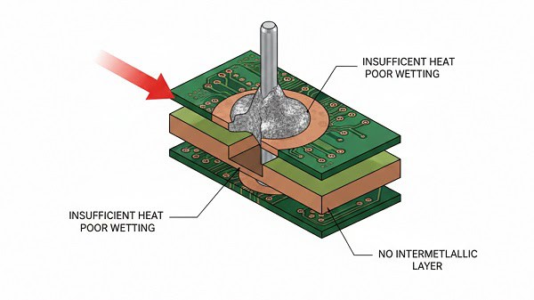
The visible defect is usually the result of a process condition rather than one universal temperature setting. The thermal mass of the board, alloy, flux chemistry, finish, component termination, stencil design, oven or iron performance, and handling history all affect wetting.
| Cause group | Examples | What to verify |
|---|---|---|
| Insufficient or uneven heat | Short contact time, heavy copper, poor tip contact, unsuitable reflow profile | Profile or tool performance at the actual joint |
| Contamination or oxidation | Oxidized pads or leads, residues, poor storage | Incoming condition, shelf life, cleaning and handling |
| Flux problem | Wrong chemistry, expired material, insufficient activity, excessive heat exposure | Approved flux, storage, application and process window |
| Mechanical disturbance | Movement before solidification, vibration during hand soldering | Fixture, operator method and cooling stage |
| Material or design mismatch | Large thermal imbalance, unsuitable pad geometry, difficult finish or termination | Land pattern, stencil, DFM and component requirements |
Reflow peak temperature, time above liquidus, ramp rate, preheat, and hand-soldering tip temperature must be set for the approved alloy and components. Treat values from a general article as starting context only; the solder paste data sheet, component limits, board construction, and measured profile control the actual process.
How to Fix a Cold Solder Joint Safely
A repair should restore wetting without damaging the pad, component, laminate, or nearby parts. If the board is powered, disconnect it and follow the product’s electrical-safety and ESD procedures. High-energy, mains, battery, medical, or safety-critical assemblies should be handled by qualified personnel.
- Document the location, failure symptom, and pre-repair inspection result.
- Remove contamination and, when required, old or excess solder using the approved method.
- Apply compatible flux and heat the pad and termination together with a clean, correctly sized tool.
- Feed only enough approved solder to form the required fillet; avoid prolonged or repeated heating.
- Let the joint cool without movement, then clean it if the flux process requires cleaning.
- Reinspect and repeat the relevant electrical or functional test. Record the repair and disposition.
If a pad is lifted, the component is heat-damaged, the joint remains unstable, or the same defect appears across a batch, stop treating it as a one-off repair. Escalate it to engineering and investigate the process. For through-hole work, the selective soldering vs. wave soldering guide explains how equipment choice changes process control.
How to Prevent Repeat Defects in Production

- Approve the solder alloy, flux, paste, surface finish, and component terminations before release.
- Measure the thermal profile on a representative assembly, especially around high-mass and temperature-sensitive locations.
- Control paste storage, thawing, mixing, stencil condition, print inspection, and open time according to supplier instructions.
- Maintain soldering tips, heaters, thermocouples, ovens, wave or selective-soldering equipment, and extraction systems.
- Train operators to heat both surfaces, avoid movement during solidification, and recognize pad or component damage.
- Define inspection and test coverage by package and risk; do not ask one method to find every defect.
- Track defects by reference designator, machine, line, lot, operator, material lot, and profile so recurrence becomes visible.
For outsourced production, request the process evidence that matches the risk: profile records, paste and alloy identity, first-article approval, AOI or X-ray disposition, repair log, and functional-test result. QueenEMS’ guides to choosing flux and PCBA testing cover those controls in more detail.
Cold Solder Joint Inspection Checklist
| Stage | Evidence to collect | Decision |
|---|---|---|
| Before repair | Photo, location, symptom, build lot and relevant test result | Confirm defect and scope |
| During root-cause review | Material identity, handling history, tool or profile record | Find process condition |
| After repair | Magnified inspection and repeated electrical or functional test | Accept, rework again, or reject |
| Batch review | Defect frequency and common machine, lot, package or operator | Contain affected units and correct process |
FAQ
Can a good lead-free solder joint look dull?
Yes. Surface brightness varies with alloy, finish, cooling, and process. Judge wetting, fillet geometry, cracks, contamination, movement, and the applicable acceptance criteria—not shine alone.
Can a multimeter prove that a solder joint is good?
No single multimeter reading proves long-term reliability. Continuity or resistance can expose some open or unstable connections, but circuit topology may hide a fault. Combine the appropriate electrical test with inspection and functional evidence.
Should every suspect joint be reheated?
No. Confirm the defect and the repair method first. Unnecessary reheating can damage pads, components, laminate, or nearby joints and can erase evidence needed for root-cause analysis.
What should a supplier provide after rework?
For controlled production, ask for the affected reference designator, reason for rework, approved instruction, operator or station, inspection result, repeated test result, and final disposition.
Conclusion
The practical test for a cold solder joint is not a single color, resistance number, or universal temperature. Confirm wetting and joint condition, choose a test suited to the circuit, repair with an approved method, and trace the result back to the process. That approach fixes the immediate failure and reduces the chance that the next batch repeats it.
Upload your files today · Free DFM check before production · Ship worldwide
Get your PCB prototypes in as fast as 24 hours. We handle FR4, Rogers, and hybrid boards up to 40 layers in volume production, with advanced builds subject to engineering review — free prototypes for 2–4 layer FR-4 boards, no minimum order.
Just upload your Gerber + BOM — we source every part, assemble, and inspect (AOI + X‑Ray) so you don't have to chase suppliers. Boards ship in as fast as 24 hours.