

Quick Answer: You can stop tombstoning by using symmetric pad designs, applying thermal reliefs with 0.2mm spokes on ground planes, and running a 60-90 second soak reflow profile at 150°C. Modifying your stencil to a 1:1 ratio for 0402 components and using a solder paste with a wide pasty range will eliminate the uneven wetting forces that cause parts to lift. Key takeaways:
- Pad asymmetry causes over 40% of tombstoning; always use IPC-7351 symmetric footprints.
- A soak reflow profile (150°C for 60-90s) balances thermal mass better than ramp-to-spike.
- Large copper pours drop heating rates by 10-15%, requiring 0.2mm thermal relief spokes.
- Anti-tombstoning paste formulations reduce borderline defect cases by 30-50%.
Table of Contents
- What Is Tombstoning in SMT?
- The Physics Behind Tombstoning
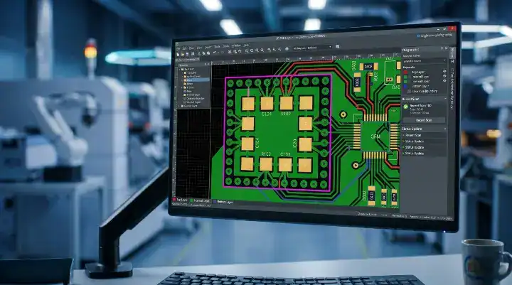
- Pad Design Considerations
- The Role of Vias
- Stencil Design Rules
- Reflow Profile Optimization
- 0402 Component Considerations
- Solder Paste Selection
- Nitrogen Reflow Effects
- Testing & Verification Methods
To stop a component from standing on one end, you must perfectly balance the thermal mass and solder wetting forces on both of its terminals. Passive components lifting vertically ruin production yields and delay shipping schedules. A 1% failure rate on a 10,000-board run means hundreds of reworked boards at $5-$15 each. We will show you exactly how to prevent tombstoning SMT using real factory data.
What Is Tombstoning in SMT?
Tombstoning is a soldering anomaly where a passive component lifts vertically off one pad, and you fix it by equalizing surface tension during reflow. Understanding how to prevent tombstoning SMT requires breaking down the mechanical forces inside your oven. Tombstoning is an imbalance defect that causes open circuits on up to 2% of unoptimized 0402 assemblies.
The Financial Impact of Defects
Here is the reality: rework destroys profit margins and threatens board reliability. Applying a manual soldering iron to a tiny 0402 capacitor risks thermal shock to the ceramic body, which means the part might fail months later in the field.
- Rework costs $5 to $15 per affected board.
- Manual heating damages adjacent microscopic components.
- Field failures from stressed parts cost thousands in warranty claims.
Root Cause Categories
Your assembly line introduces variables that trigger this lifting effect. You must control every step of the surface mount process because a failure in one area guarantees defects.
Key Takeaway: You cannot fix tombstoning by guessing; you must isolate the root cause to either layout asymmetry, paste volume, or thermal profiling. Bottom line: Audit your stencil printing first, as it causes the majority of these defects.
| Defect Root Cause | Design Fix | Process Fix | Responsible Party |
|---|---|---|---|
| Pad Asymmetry | Match pad dimensions | N/A | PCB Designer |
| Uneven Paste | Adjust aperture ratio | Clean stencil regularly | Assembly Factory |
| Thermal Imbalance | Add thermal reliefs | Use a soak profile | Designer & Factory |
Choose design fixes for permanent yield improvements, because process fixes only act as temporary patches.
The Physics Behind Tombstoning

Uneven wetting forces create an imbalanced torque during melting, causing one side to pull the component upright. The physics behind how to prevent tombstoning SMT rely entirely on fluid dynamics and surface tension. When paste melts on one pad earlier than the other, it creates an unbalanced pulling force.
The Wetting Force Imbalance
Here is the exact mechanism: liquid solder acts like an elastic band pulling on the component’s metal terminal. If pad A reaches 217°C before pad B, the solder on pad A wets the terminal and pulls backward. Because pad B is still solid paste, it offers no counter-force, resulting in the part standing up.
- Surface tension exerts 0.5 to 1.0 mN of force on a small terminal.
- Unequal heating times create a leverage effect.
- Lighter components cannot resist this torque.
Component Placement Offset
A placement machine dropping a component slightly off-center drastically changes the force distribution. The side with more terminal area resting on the paste will experience a stronger capillary pulling force.
Key Takeaway: The physical lift happens in a fraction of a second when thermal equilibrium fails, meaning your process window is incredibly tight. Bottom line: Keep the thermal mass identical on both ends of the part to balance the physical pulling forces.
| Physical Variable | Impact on Torque | Target Control Level |
|---|---|---|
| Wetting Speed | High | Slow down wetting |
| Placement Accuracy | Medium | < 0.05mm offset |
| Component Mass | High | N/A (Fixed by BOM) |
Control your wetting speed through paste selection, because you cannot change the physical mass of the components.
Pad Design Considerations
Modifying standard footprints with specific thermal reliefs on ground planes completely stops this defect. PCB designers frequently ask how to prevent tombstoning SMT when standard nominal footprints fail in production. IPC-7351 pads are a good starting point but do not account for thermal asymmetry from your custom routing.
Fixing Ground Plane Connections
Here is the exact layout rule: a pad connected directly to a large ground plane drops the local heating rate by 10-15%. You must add a thermal relief with 0.2mm spokes to restrict the heat flow. We regularly see clients struggling with this exact issue on StackExchange forums. Match your trace widths on both pads, because routing a 0.5mm trace to one side and a 1mm trace to the other creates a measurable thermal imbalance.
- Pad extensions beyond the termination must be equal (0.25-0.5mm).
- 0.2mm thermal spokes limit heat sinking to the ground layer.
- Asymmetric traces guarantee uneven reflow timing.
Factory DFM Success
At QueenEMS, we saw a client with a 5% tombstoning rate on 0402 capacitors because they skipped thermal reliefs on their ground pours. We ran their files through our free DFM engineering review and added 0.2mm spokes to their ground pads. This direct design change resulted in a 99.7% first-pass yield on their next batch of 10,000 boards.
Key Takeaway: Symmetrical copper weight around the pads is non-negotiable for small components. Bottom line: Never connect an 0402 or 0603 pad directly to a solid copper pour without a thermal relief.
| Pad Design Feature | Tombstoning Risk | Action Required |
|---|---|---|
| Solid Ground Connection | Very High | Add 0.2mm relief spokes |
| Mismatched Trace Widths | High | Equalize trace sizes |
| IPC-7351 Symmetric Pads | Low | Verify routing mass |
Use 0.2mm thermal relief spokes on all ground connections, because solid copper drains heat too fast.
The Role of Vias
Vias drain heat away from pads rapidly, so you must keep them at least 1mm away from the termination. The placement of vias heavily dictates how to prevent tombstoning SMT because they act as aggressive thermal heatsinks.
Via Proximity Rules
Here is the standard practice: placing a via directly next to a pad pulls the oven’s heat down into the internal layers. This causes the via-side pad to remain cold while the isolated pad melts and pulls the component.
- Keep all vias more than 1mm away from the component pad.
- If you must use close vias, mirror them symmetrically on both sides.
- Avoid via-in-pad for small passives unless they are fully filled and plated over.
Balancing Copper Mass
If your layout forces you to put a heavy trace on one side, you must artificially increase the copper mass on the other side. You can add a dummy trace or a blind copper pour to balance the thermal load.
Key Takeaway: Vias steal heat from the solder joint, which means they destroy the thermal equilibrium required for a flat component. Bottom line: Keep vias 1mm away from passives or mirror their placement to equalize the heat loss.
| Via Placement | Thermal Effect | Tombstone Risk |
|---|---|---|
| < 0.5mm from pad | Severe heat drain | High |
| Mirrored on both pads | Balanced heat drain | Low |
| > 1.0mm from pad | Negligible impact | Minimal |
Mirror your via placements on both sides of the component, because balanced heat loss prevents torque imbalances.
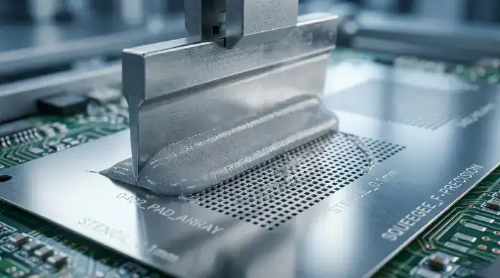
Stencil Design Rules
Applying a 1:1 aperture ratio for 0402 parts and reducing volume by 5-10% for larger components stops uneven lifting. Controlling paste volume perfectly is how to prevent tombstoning SMT on high-density layouts. Industry statistics prove that over 70% of SMT assembly defects originate from solder paste printing issues.
Squeegee and Print Settings
Here are the specific factory numbers: you must maintain a squeegee pressure of 1-3 kg/cm² and a print speed of 20-50 mm/s. Fast printing causes dog-ear shapes on the paste deposit. You must also clean the stencil every 5-10 boards to stop paste from clogging the tiny corners.
- Use a stencil thickness of 0.1mm to 0.15mm for fine-pitch boards.
- Maintain a squeegee pressure of 1-3 kg/cm².
- Wipe the underside of the stencil every 5-10 prints.
Aperture Geometries
If your stencil deposits too much paste, the surface tension force multiplies. Use a step stencil technique that is locally thicker for large components but thinner for small 0402 and 0603 parts. A trapezoidal aperture design promotes better paste release, resulting in identical paste bricks on both pads.
Key Takeaway: Uneven paste deposits create uneven pulling forces, meaning precise stencil design is your best defense against lifting. Bottom line: Use a 1:1 aperture ratio for tiny components and reduce the thickness to 0.1mm to limit excess paste volume.
| Component Size | Recommended Aperture Ratio | Risk Level |
|---|---|---|
| 0201 | 1:1 ratio | Extreme |
| 0402 | 1:1 ratio | Very High |
| 0805 / 1206 | 5-10% reduction | Medium |
Reduce your stencil aperture by 5-10% for larger components, because excess paste generates unnecessary pulling torque.
Reflow Profile Optimization
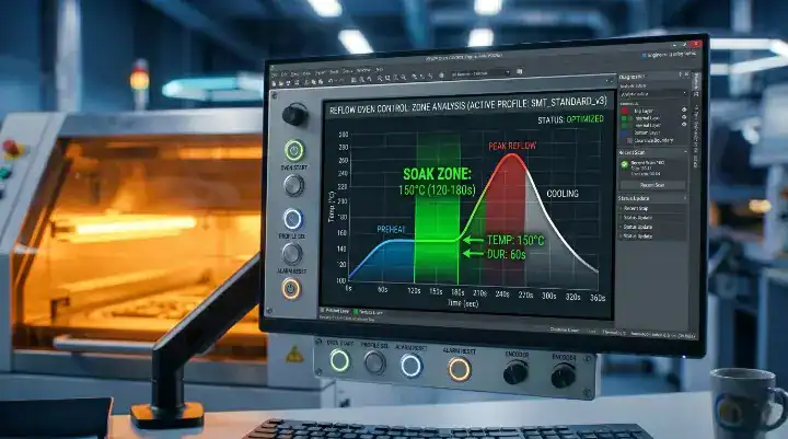
A gradual soak profile at 150°C for 60-90 seconds equalizes thermal mass better than a rapid ramp-to-spike. Adjusting the oven settings directly answers the Reddit community’s question regarding how to prevent tombstoning SMT with SAC305 alloys. Lead-free SAC305 has a narrower process window with a 217°C liquidus, making it much harder to control than old SnPb paste.
Soak vs Ramp-to-Spike
Here is the exact oven profile: a soak profile of 60-90 seconds at 150-180°C allows all parts of the board to reach the exact same temperature before melting. A ramp-to-spike profile heats too fast, causing small pads to melt while heavy ground pads stay solid. A mere 5°C temperature variation across the board will trigger tombstoning.
- Set your preheat soak at 150°C ±10°C for 60-90 seconds.
- Keep the ramp rate below 2°C/second through the liquidus zone.
- Target a SAC305 peak of 230-250°C with a TAL of 45-90 seconds.
The Liquidus Transition
Reducing the ramp rate through the liquidus zone is the single most effective reflow change you can make. When you slow down the transition, you give both pads time to cross the 217°C threshold simultaneously.
Key Takeaway: Fast heating causes thermal mismatch, which means a prolonged soak zone is mandatory for boards with diverse copper weights. Bottom line: Program your oven for a 60-90 second soak at 150°C to guarantee simultaneous paste melting.
| Reflow Zone | Temp Range / Time | Purpose / Impact |
|---|---|---|
| Soak Zone | 150-180°C (60-90s) | Equalizes thermal mass (Lowers risk) |
| Ramp to Liquidus | < 2°C / second | Prevents thermal shock (Lowers risk) |
| Peak / TAL | 230-250°C (45-90s) | Final joint formation |
Use a soak profile instead of ramp-to-spike, because it eliminates the 5°C variations that trigger component lifting.
0402 Component Considerations
Miniaturized 0402 and 0201 parts have lower mass, making them highly susceptible to unbalanced surface tension. Component mass directly dictates your strategy on how to prevent tombstoning SMT on modern boards. A heavy 1206 capacitor has enough physical weight to resist the pulling force of melting solder.
The Risk of Miniaturization
Here is the physical limitation: an 0201 component weighs almost nothing, which means even a 0.1 mN force imbalance will violently flip it upright. You must tighten your placement machine tolerances to ±0.03mm for these micro-components.
- 0201 and 0402 packages represent 90% of all tombstoning defects.
- Component metallization quality varies between cheap and premium brands.
- Poor component solderability causes one end to reject the paste.
Adjusting for Small Parts
If your components have oxidized terminals from bad factory storage, the paste will wet unevenly. You must verify the solderability of your tiny passives before loading the reels onto the machine.
Key Takeaway: Micro-components lack the gravity to stay flat, meaning your pad design and paste volume must be absolutely flawless. Bottom line: Shrink your stencil thickness to 0.1mm when dealing with 0402 parts to prevent excessive surface tension.
| Component Size | Physical Mass | Tombstoning Susceptibility |
|---|---|---|
| 0201 / 0402 | Extremely Low | Critical |
| 0603 | Low | High |
| 1206 | High | Low |
Tighten your stencil and placement tolerances for 0402 parts, because their low mass cannot resist uneven pulling forces.
Solder Paste Selection
Switching to a solder paste alloy with a wider pasty range slows wetting speeds and limits defect rates. Process engineers often debate how to prevent tombstoning SMT without changing the physical PCB layout. Solder alloys with a wider pasty or plastic range slow down the wetting action and reduce the sudden force imbalance.
Pasty Range Physics
Here is the chemistry fact: SAC305 has a near-eutectic melting point around 217°C with a very narrow pasty range. This causes it to turn from solid to liquid almost instantly, pulling the component violently. Older SnPb pastes had a wider range, making them more forgiving.
- A narrow pasty range causes instant, aggressive wetting forces.
- A wider pasty range creates a slow, forgiving transition.
- Slowing the wetting speed gives the colder pad time to catch up.
Anti-Tombstoning Formulations
Some paste manufacturers offer specific anti-tombstoning formulations that mix alloys (like adding antimony or bismuth) to deliberately widen the melting range. While paste alone will not fix a fundamental pad design asymmetry, it can reduce borderline cases by 30-50%.
Key Takeaway: Standard SAC305 melts too fast for unbalanced pads, which means specialized paste formulations act as a valuable safety net. Bottom line: Ask your assembly partner for an anti-tombstoning paste formulation if your layout contains unchangeable thermal imbalances.
| Solder Alloy Type | Melting Behavior | Tombstoning Risk |
|---|---|---|
| Standard SAC305 | Near-eutectic (Fast) | High |
| SnPb (Leaded) | Wide pasty range | Low |
| Anti-Tombstone Mix | Artificially widened | Medium-Low |
Select an anti-tombstoning paste formulation for dense boards, because it slows down the liquid transition and reduces pulling torque.
Nitrogen Reflow Effects
Using a nitrogen atmosphere increases wetting speeds, which can actually worsen tombstoning on poorly designed pads. Evaluating your oven atmosphere is a critical step in how to prevent tombstoning SMT when working with high-end military or medical boards.
The Nitrogen Dilemma
Here is the operational conflict: injecting nitrogen (N2) into the reflow oven prevents oxidation and creates brilliant, shiny solder joints. However, eliminating oxygen makes the solder paste grab the component terminal much faster and harder.
- N2 environments reduce the surface tension of the liquid solder.
- Faster wetting times exaggerate any thermal imbalances on the pads.
- Oxygen limits wetting speed, acting as a natural brake.
Atmosphere Optimization
If you suffer from high defect rates in an N2 oven, turning off the nitrogen or increasing the oxygen Parts Per Million (PPM) often solves the problem instantly. You must balance the need for pristine joints against the mechanical risk of lifting parts.
Key Takeaway: Nitrogen accelerates the melting process, which means it punishes layout asymmetries much harder than a standard air oven. Bottom line: If you experience sudden tombstoning spikes in an N2 oven, increase your oxygen PPM to slow down the wetting forces.
| Oven Atmosphere | Wetting Speed | Joint Oxidation | Tombstone Risk |
|---|---|---|---|
| Standard Air | Slow | Moderate | Lower |
| Nitrogen (N2) | Very Fast | Zero | Higher |
Use standard air reflow if your layout has severe thermal imbalances, because nitrogen makes the solder pull too quickly.
Testing & Verification Methods
Solder Paste Inspection (SPI) catches volume imbalances before reflow, while Automated Optical Inspection (AOI) catches the lifted parts afterward. Knowing how to prevent tombstoning SMT requires implementing strict inline inspection protocols to catch deviations before they become permanent.
SPI for Early Detection
Here is the quality control standard: a 3D SPI machine scans the wet paste deposit on every single pad. If the paste volume on pad A is 20% higher than pad B, the machine flags the board before the components are placed.
- SPI prevents defects by catching the root cause (paste imbalance).
- Post-reflow AOI catches the physical defect (the lifted part).
- X-ray is generally not required for this specific visible defect.
AOI and Factory Strategy
A recent customer missed paste volume errors during prototyping, resulting in a 3% defect rate. When they moved to QueenEMS, we deployed our standard 3D AOI and SPI on every board. Because we catch paste asymmetry before reflow, we saved them $12,000 in potential rework costs and achieved a 99.7% first-pass yield.
Key Takeaway: Finding a tombstoned part after reflow is too late; you must inspect the paste deposition to prevent the physical lifting. Bottom line: Mandate 3D SPI checks from your manufacturer to catch the paste volume imbalances that trigger these defects.
| Inspection Method | Detection Stage | What It Catches |
|---|---|---|
| 3D SPI | Pre-reflow | Uneven paste volume |
| 3D AOI | Post-reflow | Lifted components |
| Manual Visual | Post-reflow | Obvious severe defects |
Rely on 3D SPI to catch errors early, because adjusting the stencil printer costs nothing compared to reworking a soldered board.
Do You Need Help Stabilizing Your SMT Yields?
Fixing a tombstoning problem requires deep process engineering, not just guesswork. You need a partner who understands the relationship between pad design, stencil thickness, and soak profiles.
QueenEMS provides full turnkey service from component sourcing to final assembly, supporting prototypes up to mass production scaling. We run a free DFM and DFA engineering review on every single order to catch pad asymmetries before your boards hit the floor. Reach out to our engineering team and contact us today to stabilize your yields and eliminate rework for good.
Written by the QueenEMS Engineering Team
Frequently Asked Questions
Can I fix tombstoning by just changing my stencil thickness? Yes, in many borderline cases. Reducing your stencil thickness from 0.15mm to 0.1mm decreases the total solder paste volume. Less volume means less pulling force on the component terminal during reflow. Ask your assembly partner to run a test batch with a thinner step stencil.
What’s the best reflow profile to stop components from lifting? A gradual soak profile is the absolute best solution. You must hold the oven temperature at 150°C to 180°C for 60 to 90 seconds before ramping up to the melting point. This allows the heavy copper ground planes and the tiny isolated pads to reach the exact same temperature simultaneously.
How do I know if my PCB pad design is causing the problem? Look at your routing traces. If one pad has a tiny 0.2mm trace and the other pad connects directly to a massive solid copper pour, your design is causing the defect. The solid copper acts as a heatsink, keeping that pad cold while the other pad melts and pulls the part upright.
Can I use nitrogen reflow if my board has thousands of 0402 parts? Yes, but you must have perfect pad symmetry. Nitrogen prevents oxidation and speeds up the wetting process, which makes the solder pull the components much harder. If your layout has thermal imbalances, turn off the nitrogen to slow down the wetting forces.
What’s the best way to catch this defect before it ruins my batch? You must use a 3D Solder Paste Inspection (SPI) machine. SPI measures the exact volume of paste on every pad before the components are placed. If the machine detects an imbalance, the operator wipes the board clean and reprints it, saving you from expensive rework.
Upload your files today · Free DFM check before production · Ship worldwide
Get your PCB prototypes in as fast as 24 hours. We handle FR4, Rogers, and Flex up to 60 layers — free prototypes for 2–4 layer boards, no minimum order.
Just upload your Gerber + BOM — we source every part, assemble, and inspect (AOI + X‑Ray) so you don't have to chase suppliers. Boards ship in as fast as 24 hours.