
Quick Answer: The right PCB inspection method depends on your volume and component types. AOI costs $0.05–$0.15 per board and catches surface defects, X-ray costs $0.50–$2.00 per board to inspect hidden BGA joints, and ICT fixtures cost $2,000–$20,000 for electrical testing. For runs under 500 boards, combining AOI and flying probe testing provides >95% fault coverage without expensive fixture costs. Key takeaways:
- AOI adds $0.05–$0.15 per board and inspects 100% of visible solder joints in 10-30 seconds.
- X-Ray (AXI) costs $0.50–$2.00 per board and is mandatory for verifying void percentages under BGAs and QFNs.
- ICT fixtures run $2,000–$20,000 but test boards in 1-2 minutes, breaking even at 50-250 units.
- Flying Probe costs $1–$5 per board with zero setup fees, making it ideal for prototypes under 50 units.
Table of Contents
- What Does Each PCB Inspection Method Actually Do?
- What Defects Can AOI, X-Ray, and ICT Each Catch — and Miss?
- How Much Does Each Inspection Method Cost Per Board?
- Which Inspection Method Fits Your Production Volume?
- Do You Need X-Ray If Your Board Has BGAs or QFNs?
- Can You Combine AOI, X-Ray, and ICT — and Should You?
- How Do You Design Your PCB for Better Inspection Coverage?
- What Inspection Strategy Should You Ask Your Assembly Partner About?
- Do You Need Help Planning Your PCB Testing Strategy?
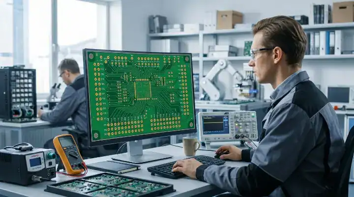
Hardware engineers often struggle to balance defect coverage with testing costs. You do not want field failures, but paying for unnecessary test fixtures ruins your project budget. At QueenEMS, our AOI vs X-Ray vs ICT layered inspection strategy maintains a 99.7% first-pass yield rate across thousands of batches. Here is exactly how to pick the right inspection protocol based on your board complexity and production volume.
What Does Each PCB Inspection Method Actually Do?
AOI uses high-resolution cameras to verify surface placements in 10-30 seconds, X-ray penetrates components to check hidden joints in 1-5 minutes, and ICT uses spring-loaded probes to verify electrical continuity in 1-2 minutes. You need to know the specific mechanics of each system to understand their limitations.
- AOI (Automated Optical Inspection) is a visual verification system checking component polarity and solder fillets at 10-30 seconds per board.
- X-Ray Inspection (AXI) is a penetration technique analyzing solder density under packages, taking 1-5 minutes per board.
- ICT (In-Circuit Testing) is an electrical verification method using a custom bed-of-nails fixture costing $2,000-$20,000 to test exact component values.
- Flying Probe is a fixtureless electrical test using robotic arms, costing $1-$5 per board and taking 2-10 minutes.
| Feature | AOI | X-Ray (AXI) | ICT (Bed of Nails) | Flying Probe |
|---|---|---|---|---|
| Detection Target | Visible surface defects | Hidden solder joints | Electrical parameters | Electrical parameters |
| Speed | 10-30 sec/board | 1-5 min/board | 1-2 min/board | 2-10 min/board |
| Setup Cost | Low (Programming only) | Low (Programming only) | High ($2,000-$20,000) | Zero fixture cost |
| Best Use Case | 100% of all PCBA runs | Boards with BGAs/QFNs | High-volume production | Prototypes / Low-volume |
Choose AOI for 100% of your visible surface mount parts as your baseline defense. Choose X-ray if your board includes bottom-terminated components like BGAs. Choose ICT if you manufacture 500+ units and need fast electrical verification.
Bottom line: Visual methods (AOI/AXI) verify physical solder quality, while electrical methods (ICT/Flying Probe) verify component functionality. You usually need both.
What Defects Can AOI, X-Ray, and ICT Each Catch — and Miss?
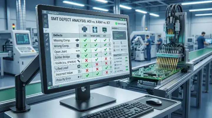
AOI catches 90% of surface defects like missing parts or solder bridges but misses hidden connections. X-ray detects 100% of BGA voids but cannot test electrical function. ICT catches wrong resistor values and shorts but requires physical test points on the board.
A common misconception in the industry is that AOI can replace electrical testing. It cannot. A resistor might look perfectly soldered to the AOI camera, but it could be completely dead internally. You must pair optical checks with electrical tests to guarantee a working product.
| Defect Type | AOI | X-Ray | ICT / Flying Probe |
|---|---|---|---|
| Missing Component | Yes | Yes | Yes |
| Tombstoning | Yes | Yes | Yes (Detects open circuit) |
| Visible Solder Bridge | Yes | Yes | Yes (Detects short) |
| BGA Solder Void | No (Blind spot) | Yes | No |
| Wrong Component Value | Sometimes (If text is visible) | No | Yes |
| Internal Chip Failure | No | No | Yes |
If you suspect a solder bridge between fine-pitch IC pins, AOI is your fast and cheap solution. If you need to verify a hidden void under a processor, you must use X-ray. If the wrong batch of capacitors gets loaded onto the reel, ICT is the only method that will reliably catch the error before shipping.
Bottom line: No single method catches everything. AOI is your baseline, X-ray handles hidden joints, and ICT catches the wrong parts loaded into the machine.
How Much Does Each Inspection Method Cost Per Board?、
AOI costs $0.05–$0.15 per board and is often included free by standard CMs. X-ray adds $0.50–$2.00 per board. ICT fixtures cost $2,000–$5,000 for simple 2-layer boards and $10,000–$20,000 for complex multilayers, plus $0.10–$0.30 per test. Flying probe has zero fixture cost but charges $1–$5 per board.
Engineers frequently debate the true cost of ICT fixtures on forums. Some report paying $2,000 for a simple fixture, while others see quotes for $20,000. You need to know the real break-even point between flying probe and ICT.
- At 500 boards, a $5,000 ICT fixture amortizes to $10 per board, making the $1–$5 flying probe cheaper.
- At 2,000+ boards, that same fixture cost drops to $2.50 per board, making ICT the clear winner.
- The industry standard break-even point usually falls between 50 and 250 boards, depending heavily on how many test nodes your board requires.
Bottom line: If you are building fewer than 250 boards, skip the expensive ICT fixture and use flying probe testing combined with AOI to save your budget.
Which Inspection Method Fits Your Production Volume?
For prototypes under 50 boards, use AOI plus Flying Probe to avoid NRE fees. For mid-volume runs of 100-500 boards, use AOI, targeted X-ray, and Flying Probe. For high-volume production over 1,000 units, invest in an ICT fixture and run AOI on every board.
Your inspection budget changes drastically based on how many boards you order. Paying a $5,000 setup fee for 10 prototype boards adds $500 to each unit. You need a volume-based strategy.
| Production Volume | Strategy Recommendation | Cost Logic |
|---|---|---|
| Prototype (<50 boards) | AOI + Flying Probe | Zero fixture costs; higher per-board test time is acceptable. |
| Mid-Volume (100-500 boards) | AOI + X-Ray (if BGA) + Flying Probe | Avoids ICT fixture risk if design changes are still possible. |
| High-Volume (1,000+ boards) | AOI + Selective X-Ray + ICT | ICT fixture cost amortizes down to <$2 per board; test speed is critical. |
Choose Flying Probe if you expect board design changes in the next 6 months, because changing an ICT fixture costs thousands of dollars. Choose an ICT fixture if your design is locked and you are scaling to thousands of units to speed up your assembly line.
Bottom line: Match your testing strategy to your batch size so you do not waste thousands of dollars on permanent fixtures for a temporary prototype.
Do You Need X-Ray If Your Board Has BGAs or QFNs?
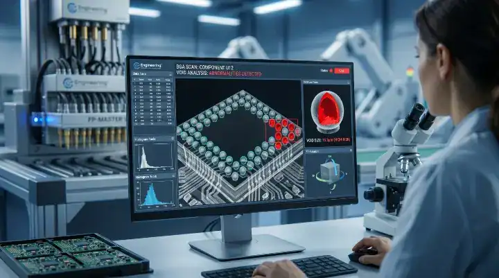
Yes, X-ray is 100% necessary for BGAs and QFNs because AOI physically cannot see solder joints hidden under the package body. X-ray adds $0.50–$2.00 per board but prevents field failures that cost $50–$500 to recall and repair.
Many engineers ask whether X-ray is really necessary for BGA boards or if AOI alone is sufficient. Some report that their CM charges extra for X-ray inspection and wonder if it is worth the cost. This is a physics limitation, not a quality gap.
- IPC-A-610 Class 3 strictly requires X-ray to verify BGA acceptance criteria.
- X-ray quantifies the exact void percentage in BGA joints, keeping it below the typical 25% void area limit.
- QFN ground pads are also hidden under the component, meaning the exact same X-ray requirement applies to them.
Bottom line: Never skip X-ray on BGA or QFN boards; visual inspection cannot verify what the camera cannot physically see.
Can You Combine AOI, X-Ray, and ICT — and Should You?
Yes, combining AOI with ICT or Flying Probe achieves >95% overall fault coverage. The recommended layered approach is SPI pre-reflow, post-reflow AOI, selective X-ray for BGAs, followed by ICT or Flying Probe.
Engineers building medical or aerospace products want to know which test combination gives the highest coverage without overkill. Some CMs push full testing suites that add unnecessary costs. You need to layer your defenses. Rule of thumb: AOI and AXI verify physical solder quality defects, while ICT and FPT verify electrical connectivity defects. They are perfectly complementary, not redundant.
| Industry | Minimum Inspection Requirements |
|---|---|
| Consumer Electronics | SPI + AOI + Flying Probe (Runs <500) |
| Industrial / IoT | SPI + AOI + X-Ray (BGAs) + ICT |
| Medical Devices | SPI + AOI + X-Ray (100%) + ICT + FCT |
| Aerospace / Defense | SPI + 3D AOI + 3D X-Ray + ICT + FCT |
If you build basic consumer gadgets, stick to AOI and flying probe to save money. If you build life-saving medical devices, use the full suite including ICT and Functional Testing (FCT).
Bottom line: Layer your inspection methods starting with SPI and AOI to catch 80% of errors early, leaving electrical testing to verify final functionality.
How Do You Design Your PCB for Better Inspection Coverage?
Design for Testability (DFT) reduces inspection costs by 20-30%. Adding test points for every net on the bottom layer reduces ICT fixture complexity and allows flying probes to test a board in 2 minutes instead of 10.
Your layout decisions directly dictate your testing bill. Clear component spacing allows AOI cameras to inspect solder fillets without shadows causing false failures. Good pad design stops tombstoning before it starts. Proper PCBA testing relies heavily on how well you place test nodes during the layout phase. If a net has no test point, the flying probe has to touch the component leg directly, which drastically slows down the machine and risks physical damage.
Bottom line: Add accessible test points to every net on a single side of the board during layout to dramatically lower your electrical testing costs.
What Inspection Strategy Should You Ask Your Assembly Partner About?
Ask your CM if they run 3D AOI and provide automated SPI before reflow. Standard 2D AOI misses up to 15% of volumetric solder defects that modern 3D systems catch easily.
We see clients struggling with high defect rates from cheap assembly houses. They pay low upfront prices but lose weeks dealing with RMAs. At QueenEMS, our standard practice includes 3D AOI and 100% X-ray inspection on every BGA assembly. Because we verify every hidden joint with precise volumetric data, we achieve a 99.7% first-pass yield rate for our clients. You should expect this level of data transparency from your manufacturing partner.
Bottom line: Demand a documented inspection flow from your assembly partner that clearly separates visual verification steps from electrical testing steps.
Do You Need Help Planning Your PCB Testing Strategy?
Resolving the AOI vs X-Ray vs ICT debate comes down to knowing your board complexity, your component types, and your exact order volume. You do not have to figure out the break-even math alone.
QueenEMS provides full turnkey service from component sourcing to final testing, making certain every board meets IPC standards before it ships. We offer a free DFM and DFT engineering review on every order to catch testing bottlenecks before fabrication begins. Reach out to our engineering team and contact us today to discuss the perfect inspection strategy for your next batch.
Written by the QueenEMS Engineering Team
Frequently Asked Questions
Can AOI completely replace ICT? No. AOI only verifies visual surface features like part presence and solder shape. It cannot check if a resistor has the wrong internal value or if a hidden trace is broken. Always pair AOI with an electrical testing method. If you want high coverage, talk to your CM about adding flying probe testing.
What is the cheapest way to test 20 prototype boards? The cheapest method is combining standard AOI with Flying Probe testing. You pay $1–$5 per board for the electrical test but completely avoid the $2,000+ setup fee required for an ICT bed-of-nails fixture. Check if your manufacturer offers in-house flying probe services for small runs.
Does X-ray testing damage sensitive components? No. The radiation dose from a standard 1-5 minute 2D or 3D X-ray inspection is far too low to damage standard silicon components. It is entirely safe for modern microcontrollers, memory chips, and passive components. If you have extremely sensitive specialized sensors, share your BOM with your assembly partner to verify safety limits.
QueenEMS Sales
Online · Replies in minutes