

Quick Answer: Hybrid PCB layer registration should be controlled through agreed design margins, material-specific CAM compensation, in-process targets, and measurable acceptance evidence. Buyers should not copy one universal alignment number into every RFQ; they should identify the features that are sensitive to misregistration, ask how the supplier will verify them, and tie the report to the released stackup and lot.
Key takeaways
- Registration is a chain that includes inner-layer imaging, core movement, lamination, final drilling, and outer-layer alignment.
- PTFE and FR4 can move differently, so a supplier’s standard multilayer capability does not automatically prove the hybrid construction.
- The design margin around holes, pads, reference planes, cavities, and RF launches should drive the evidence request.
- X-ray targets, coupons, microsections, and dimensional reports answer different questions and should not be treated as interchangeable.
Layer registration becomes an order-stage problem when a small positional shift can break an annular ring, change a reference-plane relationship, move a drilled feature toward copper, or misalign an RF transition. A supplier may be able to build the board, yet still need more margin or a revised inspection plan before the quote is defensible.
For hybrid PCB layer registration, material behavior is part of the alignment budget. Low-loss laminates, bonding layers, and FR4 cores can have different dimensional movement through imaging and lamination. The buyer does not need to calculate the factory’s scale factors, but the RFQ must show which relationships are critical and what proof will be returned.
This page is narrower than a general hybrid stackup RFQ. It focuses on how engineering and quality define, inspect, and approve positional relationships after the material construction is selected.
Table of Contents
- Define which registration relationship matters
- Build margin from the released geometry
- Ask how mixed materials will be compensated
- Select evidence for the feature at risk
- Set the sampling and report scope
- Separate design nominal from acceptance data
- Review exceptions before fabrication proceeds
- Create a registration-ready RFQ package
Define which registration relationship matters
Registration is not one measurement. It can describe inner pattern to inner pattern, one core to another core, outer pattern to inner features, final drill to internal lands, solder mask to copper, or routed outline to a connector footprint. Each relationship is created and verified at a different point in fabrication.
Begin by naming the consequence of movement. A dense plated hole may lose land. A ground aperture may shift relative to an RF via. A cavity may approach internal copper. A connector launch may lose symmetry. A broad statement such as “tight layer registration required” does not tell the fabricator where to spend margin or what the buyer will inspect.
Map the sensitive feature to its datum and layer pair. If a hole must land on L3 and L6, show the target lands and clearance on those layers. If an RF launch depends on a top trace, internal reference plane, and board edge, show all three relationships. That map becomes the basis for DFM and evidence.
| Relationship | Typical failure if it shifts | Useful drawing callout |
|---|---|---|
| Drill to inner land | Annular ring loss or breakout | Hole, target pad, and approved compensation |
| Plane opening to via | Reduced clearance or RF discontinuity | Aperture size and affected layer |
| Inner layer to inner layer | Coupling or connection change | Critical overlap and datum |
| Board edge to RF launch | Connector fit or return-loss variation | Edge profile, launch geometry, and thickness |
Scope rule: Define registration by the two features that must align and the consequence of their movement, not by one unexplained tolerance note.
Build margin from the released geometry
The safest registration control begins in the design. Pad size, annular ring, antipad clearance, copper-to-edge distance, cavity keepout, and connector landing geometry create the available process window. A drawing that leaves no manufacturing margin cannot be rescued by asking for an aggressive capability number after routing is complete.
Ask the fabricator for a DFM view of the worst layer pair, not only the average feature. Inner layers can have different pad or clearance geometry, and the most constrained land may be hidden in a dense transition. For holes, finished diameter, drill diameter, plating allowance, drill wander, and layer movement all contribute to the available ring.
Use the PCB board outline tolerance requirements page when the critical relationship ends at a routed edge. Use copper-to-edge clearance requirements when internal or external copper approaches the profile. This article covers the alignment chain between those controlled features.
Design margin should also reflect quantity and learning stage. A one-panel prototype may be useful for confirming the concept, but a production release needs geometry that remains manufacturable across normal material lots, panels, tooling, and operators. Do not qualify a zero-margin design merely because one sample happened to land well.
Margin signal: If the supplier must rely on perfect alignment rather than a defined process window, the layout should return to engineering before the PO is released.
Ask how mixed materials will be compensated
Inner layers change dimension during processing. Imaging, etching, baking, resin flow, pressure, temperature, copper distribution, and material construction can all affect the final position of targets. Fabricators use measured history and in-process data to scale or compensate artwork and drilling for a given material system.
Hybrid boards deserve a separate review because the low-loss and FR4 portions may not follow the same movement pattern. A compensation developed for a standard FR4 stack should not be assumed to represent a PTFE/FR4 construction. The supplier should review layer symmetry, copper balance, material orientation, panel layout, and the order in which subassemblies are pressed.
The buyer should ask three practical questions: Has the exact material pairing been reviewed? Which in-process targets will show actual movement? How will final drill or imaging be aligned to the laminated panel rather than only to nominal CAD coordinates? These questions request evidence without demanding confidential scale factors.
The hybrid lamination and CTE article explains the material-behavior boundary. Registration uses that information to decide whether lands, apertures, and drilled features will still overlap after the press cycle.
| Supplier control | What it manages | Buyer-facing output |
|---|---|---|
| Inner-layer target measurement | Actual layer or core movement | DFM confirmation or process record |
| CAM scaling by material set | Predictable dimensional change | Approved processed data |
| Lamination pinning or optical alignment | Layer placement during pressing | In-process conformance record |
| X-ray target drilling | Final drill position to internal targets | Measurement or inspection result |
Compensation check: Ask how the supplier converts actual panel movement into aligned drilling and imaging; do not ask for a generic machine accuracy figure.
Select evidence for the feature at risk
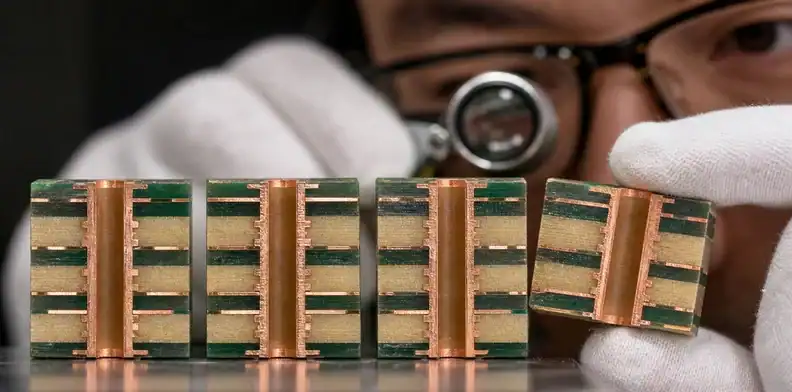
Inspection should follow the hidden relationship. Optical inspection can evaluate exposed artwork or mask alignment, but it cannot directly show every internal layer after lamination. X-ray targets can help locate internal features relative to a drill or another target. A microsection can show a local hole-to-land relationship and the finished plated construction. Coupon and panel measurements may show process stability across selected locations.
No single image proves the whole board. A cross-section is local and destructive. An X-ray view depends on feature contrast, setup, and interpretation. A dimensional report can show selected measurements without showing every internal copper relationship. The quality plan should combine methods in proportion to the product risk.

Set the sampling and report scope
For a first lot, request evidence at the locations that challenge the process: the smallest inner land, the longest material span, the tight RF transition, or the edge feature with the least remaining clearance. Repeat lots can use the approved baseline and the agreed sampling or process-control record unless a material, stackup, panel, or factory route changes.
The PCB incoming inspection page helps translate supplier reports into receiving actions. Registration evidence should tell receiving whether to accept, hold, or escalate the lot—not merely add another PDF to the shipment.
Evidence point: Choose the inspection method by the hidden feature and decision it must support, then record the location and datum in the report request.
Separate design nominal from acceptance data
CAD coordinates describe design intent. Manufacturing measurements describe where features were produced. The approval package must keep those two data types distinct so a supplier does not present a nominal drawing value as if it were a measured result.
Ask the report to identify the measured characteristic, nominal value or target relationship, allowed range from the drawing or specification, actual result, measurement method, location, and disposition. When multiple panels or coupons are sampled, results should retain their panel or lot identity rather than being averaged into one number that hides spread.
Do not create false precision. The drawing should use units and decimal places that match a real functional requirement. If the design only needs the via to retain an acceptable land, a functional acceptance note may be clearer than an arbitrary positional figure copied from a different technology. Where the position itself controls RF or mechanical performance, document the actual datum and method.
| Report field | Why it matters | Weak alternative |
|---|---|---|
| Drawing revision | Ties result to released geometry | Filename without revision |
| Feature and layer pair | Defines what was measured | “Registration passed” |
| Actual result and range | Supports disposition | Nominal value only |
| Method and location | Makes the data interpretable | Unlabeled screenshot |
| Lot or panel identity | Supports traceability | Detached sample image |
Record rule: Acceptance data must state what was measured, where it was measured, and which released requirement produced the pass or fail decision.

Review exceptions before fabrication proceeds
A supplier may discover that a target land is too small, a plane opening needs more clearance, a panel scale differs from expectation, or a routed edge relationship leaves too little margin. That is a useful DFM finding, not a reason to hide the change inside processed artwork.
The response should show the affected layer, original geometry, proposed change, functional consequence, and any cost or schedule effect. Engineering decides whether the electrical or mechanical intent remains intact. Quality decides whether the acceptance record changes. Purchasing confirms the revised scope. The supplier should not proceed on a critical geometry change until the named owner approves it.
| Registration finding | Engineering decision | Quality decision | Purchasing action |
|---|---|---|---|
| Reduced drill-to-land margin | Confirm electrical and reliability intent | Set evidence or disposition | Hold PO release |
| Changed plane opening | Approve RF or clearance effect | Update controlled acceptance record | Accept revised scope only after approval |
| Different CAM compensation route | Confirm geometry remains within authority | Verify report method and traceability | Record the supplier assumption |
| Board-edge relationship at risk | Confirm connector or cavity fit | Define dimensional evidence | Resolve cost and lead-time effect |
Use PCB deviation request approval when a proposed condition falls outside the released requirement. Use processed Gerber approval for CAM output that preserves agreed intent but still needs controlled review.
At QueenEMS, we find that a short annotated comparison is easier to approve than a long email. A layer snapshot, measurement or clearance callout, reason for change, and clear “approve/hold” question gives the customer’s engineer enough context without exposing unrelated production details.
Approval call: Let CAM compensate within an agreed boundary, but route any change to functional geometry or acceptance evidence back to the named buyer owner.
Create a registration-ready RFQ package
Send fabrication data, NC drill and rout data, the controlled stackup, material callouts, finished thickness, via table, impedance requirements, drawing datums, critical layer relationships, quantities, acceptance specification, and requested inspection outputs. Add a simple marked image when one RF launch, connector, cavity, or dense via field controls the risk.
Ask the supplier to return the proposed stackup, material availability, registration DFM findings, CAM compensation boundaries, inspection method, sampling plan, and any geometry change before production. The reply should state which evidence will ship with the lot and which records remain internal.
For a new hybrid construction, connect this package to supplier stackup signoff and the first-article decision. For repeat orders, keep the approved drawing, processed data, material set, inspection plan, and deviation history together. A reorder should not reopen the registration basis unless one of those controlled inputs changes.
A practical note can read: “Review registration for the marked drill-to-land, plane-opening, and board-edge relationships in the attached hybrid stackup. Confirm the proposed compensation and inspection method. Provide measured first-lot evidence tied to the drawing revision, and hold for approval before changing pads, apertures, datums, layer order, or material.”
That wording gives the supplier room to use its validated controls while giving the buyer a measurable release condition.

FAQ
Is layer registration the same as drill position?
No. Drill position is one relationship within the registration chain. Layer registration can also involve pattern-to-pattern, core-to-core, outer-to-inner, solder-mask-to-copper, and routed-edge relationships.
Should I put one registration tolerance on the drawing?
Only when it describes a real functional requirement with a defined datum and measurement method. Otherwise, define the critical geometry and applicable acceptance specification, then review the supplier’s process window.
Can X-ray prove every layer is aligned?
No. X-ray is useful for selected hidden targets and features, but coverage and interpretation depend on the structure and method. Combine it with appropriate coupons, dimensional data, microsection, or process records when the risk requires them.
When should registration be requalified on a repeat order?
Revisit the evidence when the stackup, material family, layer geometry, panel, tooling, manufacturing route, supplier location, or critical acceptance requirement changes. Stable repeats can follow the agreed control and sampling plan.
Send QueenEMS a registration-ready hybrid PCB package
If your PCB or PCBA project has mixed low-loss and FR4 materials with critical drills, RF transitions, cavities, or board-edge relationships, send QueenEMS the released fabrication data, stackup, marked critical features, quantities, and evidence requirements through the contact page. We can review the registration boundary, return open DFM questions, and include the agreed inspection scope in the quotation.
Sources
Written by the QueenEMS Engineering Team
Upload your files today · Free DFM check before production · Ship worldwide
Get your PCB prototypes in as fast as 24 hours. We handle FR4, Rogers, and Flex up to 60 layers — free prototypes for 2–4 layer boards, no minimum order.
Just upload your Gerber + BOM — we source every part, assemble, and inspect (AOI + X‑Ray) so you don't have to chase suppliers. Boards ship in as fast as 24 hours.