
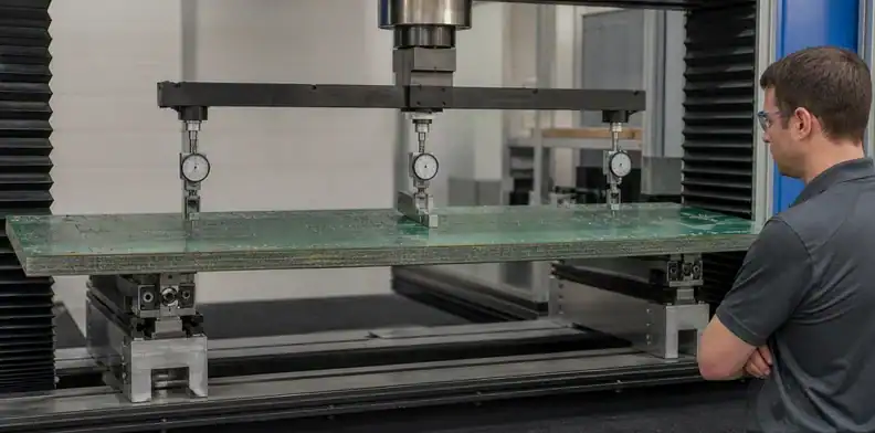
Quick Answer: Choose large PCB thickness from supported span, component weight, connector geometry and enclosure fit. A thicker board can reduce elastic sag, but it also changes stack-up, drilled-hole geometry, card-guide fit, material use and assembly tooling. Approve the value only after a production-representative mechanical and manufacturing review.
“Make the board thicker” sounds like a simple answer to flex. On an oversized PCB, it may reduce elastic sag while introducing a press-fit mismatch, a card-edge problem, a heavier carrier, longer drill geometry or a stack-up that no longer supports the original impedance plan. It may also leave the real load path unchanged if heavy components sit far from every mounting point.
Choosing thickness means balancing stiffness against connector fit, stack-up constraints and cost. For process-induced bow and twist, the large PCB warpage discussion explains copper balance and stack-up symmetry. The stiffener comparison considers rails, frames and backing structures when extra laminate thickness may not solve the support problem.
Table of Contents
- Start with span and boundary conditions
- Separate elastic stiffness from warpage
- Translate thickness into a manufacturable stack-up
- Protect connectors, holes and enclosure fit
- Model weight, handling and assembly support
- Compare thickness with local reinforcement
- Validate the selected construction
- Quote thickness without hidden assumptions
Start with span and boundary conditions
Large PCB thickness should be chosen from the actual unsupported geometry and loads. A long board supported continuously on rails behaves differently from the same outline held at four corners, and a bare-board bend test does not represent a populated assembly carrying transformers, heat sinks or insertion loads.
Draw the support condition before selecting a number
Mark every mounting hole, rail, card guide, chassis boss, connector restraint and temporary manufacturing support on the mechanical model. Then identify spans between supports and features that apply force: press-fit connectors, cable pull, mating cycles, test probes, service access and heavy parts.
The useful input is not “board is 800 mm long.” It is “a 320 mm bay between supports carries this component mass and sees this connector load.” That description lets mechanical engineering compare laminate thickness, support spacing and reinforcement without assuming that the full outline bends as one free plate.
Include load direction and life-cycle events
Gravity may act normal to the PCB in a horizontal installation or along its plane in a vertical card cage. Shipping shock, rack insertion and service handling create different load directions again. A thickness that looks sufficient in the final enclosure can still be too flexible for unrestrained work-in-process transfer.
List the conditions that matter: bare-board handling, SMT printing, reflow, test-fixture loading, connector mating, normal operation, transportation and maintenance. Engineering can then decide which event sets the design case and whether a temporary carrier solves a manufacturing-only problem more efficiently than permanent laminate thickness.
Separate elastic stiffness from warpage
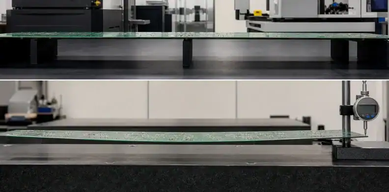
Greater thickness generally makes a plate harder to bend elastically, but it does not guarantee a flatter finished PCB. Warpage also comes from material anisotropy, copper imbalance, resin/glass distribution, lamination stress, moisture and thermal history.
| Observation | What extra thickness may do | What it cannot prove |
|---|---|---|
| Board sags under its own populated mass | Reduce elastic deflection | Eliminate residual lamination stress |
| Connector insertion bends a local bay | Improve local resistance if the load path reaches supports | Protect solder joints without nearby restraint |
| Bare board twists after fabrication | Add resistance to deformation | Correct an asymmetric construction |
| PCBA changes shape during reflow | Alter stiffness through the thermal cycle | Equalize hot and cold zones by itself |
| Board moves under ICT probe force | Reduce global flex | Replace fixture support beneath probe fields |
A thicker unbalanced board can remain warped; a thinner balanced board with well-placed supports can perform better in the product. Release thickness together with copper-balance review, flatness criteria and the installed support concept.
Decision point: Select thickness against a named span, load and support state rather than the finished outline alone.
Translate thickness into a manufacturable stack-up
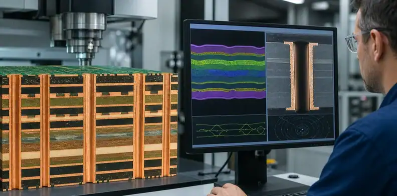
Finished thickness is the result of copper, core and prepreg choices under manufacturing tolerance. It cannot be increased independently after the electrical stack-up is complete.
Rebuild impedance and dielectric decisions
Changing core or prepreg thickness alters trace-to-plane spacing, impedance geometry, plane capacitance and sometimes routing availability. The fabricator may compensate with trace width, copper thickness or alternate glass styles, but those changes require engineering approval when they affect controlled impedance or loss.
Ask for a proposed production stack-up showing material family, core/prepreg construction, copper weights, nominal finished thickness and tolerance. Compare it with the impedance table and mechanical interfaces before approving the quotation. The supplier stack-up signoff process provides the correct background for this release.
Check drilling and lamination consequences
More thickness increases the through-hole aspect ratio for a fixed fabrication drill diameter. The finished plated-hole diameter on the drawing is a different value. AMD’s UG1099 design guidance distinguishes the finished and actual drill diameters when relating hole geometry to board thickness.
As an illustrative screening calculation, a 2.4 mm board with a 0.30 mm fabrication drill has an 8:1 ratio; increasing the board to 3.2 mm raises it to about 10.7:1. Neither result approves a construction. Ask the fabricator to confirm its drill diameter, plating allowance and qualified process limit, while retaining the connector’s finished-hole requirement unless product engineering approves a revision. Blind and buried holes need their own depth and process review.
Do not infer drill capability from layer count alone. Give the supplier the complete hole table with finished sizes, plating requirements, tolerances, via fills and backdrill definitions. If a selected thickness makes a critical hole marginal, engineering must decide whether to enlarge it, change the interconnect, use a different build structure or keep the original thickness with mechanical support.
Protect connectors, holes and enclosure fit
Board thickness is an interface dimension wherever the PCB enters a connector, guide, slot, housing or press-fit system. A mechanical gain is not useful if the assembly no longer fits or the connector loads the board incorrectly.
Card edges and guides have a mating window
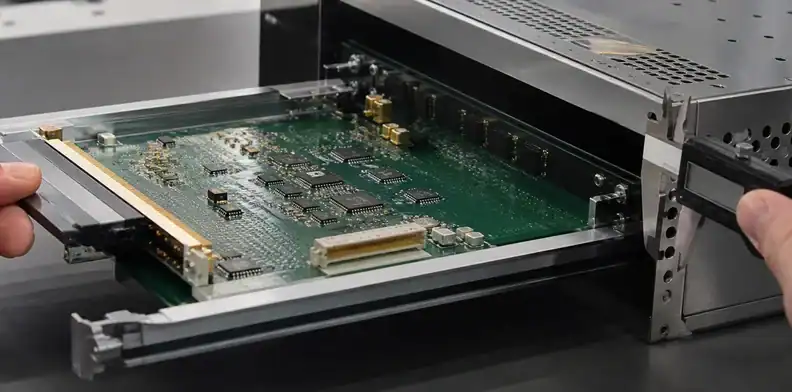
Edge-card connectors specify a compatible board-thickness range, and chassis guides or retainers have their own clearances. Surface finish and bevel geometry also matter at a card edge. Put the nominal thickness and tolerance on the interface drawing, not only in a general fabrication note.
For a large card with connectors at opposite ends, tolerance accumulation and board shape can affect insertion even when thickness is individually acceptable. Review guide spacing, parallelism, bevels and the installed restraint scheme with the enclosure model.
Press-fit and mechanical holes need a fresh review
A thickness change can affect the press-fit assembly’s required barrel geometry, support and insertion setup; compliant-pin engagement must be checked against the connector drawing rather than inferred from board thickness alone. Hole finish, copper thickness, finished diameter and connector supplier requirements remain controlling inputs. The press-fit hole tolerance review should be reopened when thickness changes.
Mounting hardware may need different standoff heights, screw lengths or shoulder geometry. Confirm underside clearance and compression stops so tightening does not bow the PCB. A washer or spacer cannot be added casually near traces, planes or bottom-side components.
Fabrication rule: Reopen stack-up, impedance and hole feasibility whenever finished thickness changes.
Model weight, handling and assembly support
Extra laminate and copper increase board mass, which changes operator handling, carrier loading and the forces acting on supports. The change can partly offset the stiffness benefit if the board still spans long distances without restraint.
Compare bare and populated mass, center of gravity and carrier capacity. A thicker board may need a revised two-person lift or full-span tray, especially after heavy parts are fitted. Printer support pins, placement rails, reflow carriers and test fixtures should be checked against the new thickness and weight rather than inherited from an earlier revision.
Assembly equipment also has thickness windows. Clamps, conveyor rails, board supports and loaders may accept the XY outline but reject a thicker edge or a heavier carrier-plus-board combination. Add the revised construction to the large-format assembly route review before approving material procurement.
Receiving inspection should distinguish nominal thickness, local thickness variation and board shape. Measure with the agreed method and support condition; do not press a bowed board flat and record the compressed result as if it represented free-state thickness.
Compare thickness with local reinforcement
The best structural solution may be thicker laminate, closer supports, a local rail, a frame, a backing plate or a combination. Compare them against the load location and product constraints rather than assuming the PCB alone must carry every force.
Use thickness for distributed stiffness
Increasing laminate thickness suits designs where stiffness is needed across much of the area, interfaces accept the change and electrical/drill consequences remain manageable. It avoids separate hardware but adds material everywhere, including regions that may not need it.
Thickness is less efficient when one connector, transformer or unsupported cutout creates a local problem. Moving a chassis boss or adding a short rail near that load can reduce flex without changing every via and card-edge interface.
Use reinforcement for a defined load path
A stiffener or frame can react connector insertion, support a heavy component or bridge a cutout while preserving the electrical stack-up. It adds parts, fasteners, keep-outs, assembly steps, mass and possible thermal-expansion stress. The support must not cover test points, obstruct rework or short copper features.
| Decision factor | Thicker laminate tends to fit | Local support tends to fit |
|---|---|---|
| Load distribution | Broad, distributed bending | Concentrated or regional load |
| Electrical stack-up | Can be revised safely | Must remain unchanged |
| Connector interface | Accepts new thickness | Fixed card-edge or pin geometry |
| Service access | No added hardware desired | Frame/rail remains accessible |
| Manufacturing issue only | Permanent stiffness still useful | Temporary carrier may be enough |
For a contextual mechanical review, provide the board model, support coordinates, mass map and interface loads through the QueenEMS DFM review. The desired output is a comparison of stack-up change versus support change, with the affected fabrication and assembly steps identified.
Evidence check: A nominal thickness value does not prove installed stiffness without shape and load measurements.
Validate the selected construction
Validation should reproduce the loads and process states that drove the thickness decision. A single flatness reading on an unloaded bare board is not enough.
Build the first article with the intended stack-up, copper distribution, surface finish, routed outline and critical holes. Record finished thickness at agreed locations, bow/twist in the defined support state, connector fit, chassis engagement and any press-fit insertion evidence. After assembly, repeat the relevant shape and fit checks with representative components and hardware installed.
| Validation state | Measurement or check | Failure exposed |
|---|---|---|
| Free bare board | Thickness map, bow and twist | Laminate or process shape outside the drawing |
| Supported bare board | Deflection at defined loads | Span too flexible for handling or probing |
| Populated assembly | Shape, connector fit and carrier contact | Component mass or reflow changes the condition |
| Installed product | Rail engagement, fastener seating and service load | Enclosure restraint hides stress or poor fit |
The same drawing revision and support definition must follow all four states. Otherwise a flat free board, a forced-flat assembly and an installed product are being compared as though they were the same mechanical condition.
Manufacturing validation may include printer support, conveyor transfer, loaded reflow, AOI access and test-fixture loading. Product validation may include cable pull, mating cycles, vibration or service forces as required by the application. These are project-specific engineering decisions; the fabricator should not invent acceptance limits when the drawing is silent.
Release the result as a construction baseline: approved stack-up revision, thickness requirement and tolerance, support hardware revision, measurement method, first-article record and authorized deviations. A later material, copper or support change should trigger a documented impact review.
Repeat the comparison at the extremes of finished-thickness tolerance. The thinnest acceptable board may govern deflection and connector support, while the thickest condition may govern card-guide insertion, rail clearance or compliant-pin engagement. Reviewing only the nominal CAD solid hides both risks. Where structural simulation is used, preserve the laminate-property assumptions and correlate at least one predicted response with physical measurement before treating the model as a release tool.
Quote thickness without hidden assumptions
Requesting only “2.4 mm PCB” leaves suppliers to guess at tolerance, stack-up, hole feasibility and mechanical intent. A comparable quotation ties the finished-thickness requirement to the complete product and process package.
Send the Gerber or ODB++ data, stack-up proposal or electrical requirements, finished thickness and tolerance, material family, copper weights, hole table, impedance table, outline model, connector specifications, support points, bare/populated mass, quantity and required evidence. Mark thickness-sensitive features such as card edges, guides, press-fit areas and controlled standoff heights.
Ask the quotation to separate material/build impact, drilling or special-process impact, tooling/support changes and validation evidence. QueenEMS can review whether the requested construction stays inside a practical fabrication and assembly route and identify where an alternate stack-up or mechanical support needs approval.
Quotation request: Use the QueenEMS oversized-board enquiry to provide the released stack-up, thickness tolerance, critical-hole table, connector interfaces and mechanical support model. The supplier response should identify the proposed construction, affected process limits and first-article measurements needed to release the chosen thickness.
Release rule: Approve the construction only after tolerance extremes remain compatible with connectors, rails and mechanical performance.
FAQ
Does a thicker large PCB always warp less?
No. Greater thickness can reduce elastic bending, but copper imbalance, material construction, lamination stress, moisture and thermal gradients can still produce bow or twist.
Is 1.6 mm suitable for every large PCB?
No. Suitability depends on unsupported span, support locations, component mass, connector forces, installation orientation and process handling. The familiar nominal value is not a structural qualification.
Will doubling thickness make a board twice as stiff?
No simple production rule should be used without the actual geometry and material properties. Plate bending stiffness changes strongly with thickness, but cutouts, anisotropic laminate, copper distribution, supports and concentrated loads alter the assembled behavior.
Can a thicker board create via problems?
Yes. At a fixed fabrication drill diameter, greater through-hole depth increases aspect ratio. Confirm the supplier’s drill and plating allowances separately from the specified finished-hole diameter, and review the affected via or connector construction before changing thickness.
Should I choose a thicker PCB or a metal stiffener?
Choose thickness for broad distributed stiffness when interfaces and stack-up can change; choose local reinforcement when a defined load path needs support or the electrical construction must remain fixed. Validate either choice in the actual assembly.
Sources
- Cadence: To Design for PCB Thickness
- iNEMI/APEX: Impact of PCB Manufacturing, Design, and Material to PCB Warpage
Written by the QueenEMS Engineering Team
Upload your files today · Free DFM check before production · Ship worldwide
Get your PCB prototypes in as fast as 24 hours. We handle FR4, Rogers, and hybrid boards up to 40 layers in volume production, with advanced builds subject to engineering review — free prototypes for 2–4 layer FR-4 boards, no minimum order.
Just upload your Gerber + BOM — we source every part, assemble, and inspect (AOI + X‑Ray) so you don't have to chase suppliers. Boards ship in as fast as 24 hours.