
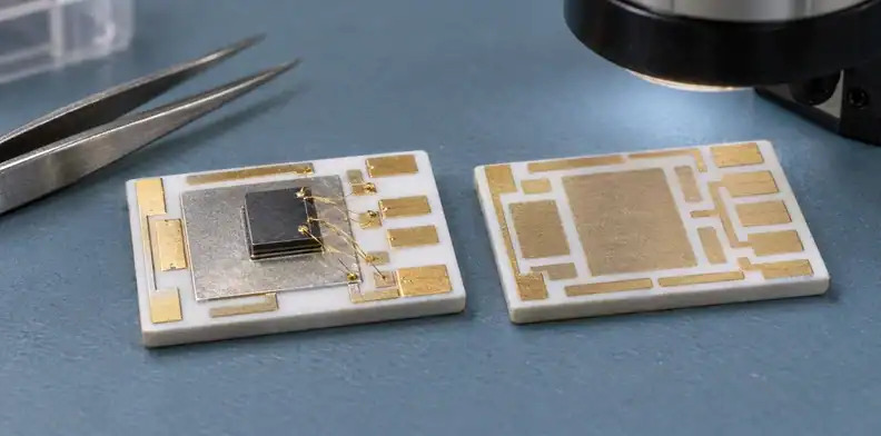
Quick Answer: Choose a ceramic PCB surface finish for the joining process at each location: wire-bond lands, sintered die lands, solder terminals and the backside interface may need different surfaces. Specify the complete metal stack, wire or paste system, functional boundaries and preceding assembly exposures. A plating-thickness report supports the finish specification; bonding and sintering still need trials on the intended construction.
A ceramic PCB surface finish should be selected alongside the wire-bond and die-attach processes. A drawing that says only “gold finish” leaves the assembler to resolve the deposited metals, local surface condition and previous thermal exposure after substrates have already been purchased.
The useful decision starts with the physical interfaces. A power die can sit on a silver-finished land while nearby wire lands need another qualified surface, and the back face can meet a third requirement. Resolve these interfaces in the fabrication drawing and trial plan before releasing a ceramic order.
Table of Contents
- What does ceramic PCB surface finish actually specify?
- Map the die, bond lands and backside separately
- Which surface can accept the specified bonding wire?
- Select the silver paste before freezing the finish
- Qualify bond lands after the preceding heat exposure
- How roughness and support change the interface
- Keep earlier assembly steps off the bond lands
- Write a finish drawing that CAM can quote
- Separate plating measurements from assembly validation
- Send a ceramic interface package for quotation
What does ceramic PCB surface finish actually specify?
Ceramic PCB surface finish specifies the exposed surface used by the next attachment, contact or protection process. It is a separate choice from the method used to put a conductor on ceramic. Direct bonded copper (DBC), active metal brazing (AMB) and direct plated copper (DPC) describe construction routes; they do not completely identify the finished bonding surface.
Start with a cross-section that identifies the exposed layers. The following layers answer different questions, even when purchasing receives them as one substrate part number.
| Part of the construction | Question it answers | Detail to identify |
|---|---|---|
| Ceramic body | Which insulating circuit carrier is specified? | Material grade and finished thickness |
| Conductor-to-ceramic system | How is the circuit metal attached or formed? | Bonding, brazing, deposition or fired-film route |
| Circuit conductor | Which metal carries the current? | Copper or the named conductor system and geometry |
| Exposed finish | What surface meets the wire, paste or solder? | Deposited layer sequence and applicable regions |
| Assembled joint | What connects the device to that surface? | Wire, sinter paste, solder or another defined attachment |
Ask the fabricator to identify the offered construction in this order. The ceramic manufacturing process comparison covers the routes themselves; the finish decision then follows the selected assembly interfaces.
For example, Rogers describes bare copper as a normal supplied surface for its curamik DBC and AMB products and lists additional finishes as options. Construction and finish are separate specifications in this example; verify the supplied surface with each fabricator. See its surface-option discussion.
A fired conductor also deserves its own material designation. The thick-film and thin-film ceramic comparison addresses that choice. Evaluate a silver-bearing fired conductor as its actual material system. Its designation does not identify a plated silver surface.
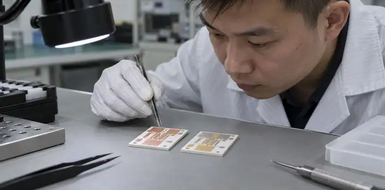
Map the die, bond lands and backside separately
Assign a surface requirement to each functional area before deciding whether the whole ceramic substrate can use one finish. A selective finish becomes useful when a common coating cannot satisfy all the intended interfaces under their qualified processes.
Frontside attachment and bond lands
Mark the die footprint, wire landing areas and solder terminals on the circuit drawing. Show both the die outline and the space occupied by attachment material after deposition and placement. Wire lands need an identifiable region that remains available when die attachment is complete.
Rogers describes whole-surface or chip-area silver plating selected according to the interconnection technology. This supports evaluating selective coverage, but it does not establish that the same silver deposit accepts every wire or paste. Ask the assembly owner to nominate a candidate surface for each operation before the fabricator proposes how to produce the boundaries.
| Functional area | Main interface decision | Drawing or process input |
|---|---|---|
| Die land | Sinter paste or solder against substrate finish | Die backside metal and attach-material designation |
| Wire land | Wire against the exposed deposited surface | Wire alloy, diameter and bonding method |
| Terminal land | Solder, weld or other terminal connection | Terminal construction and joining sequence |
| Backside attachment area | Substrate against baseplate or cooler interface | Attach material or thermal-interface arrangement |
| Uncoated ceramic region | Where metal or attachment material must stop | Dimensioned exclusion area |
The map exposes mixed-use areas early. A terminal solder operation next to a future bond land requires review of both the joining surface and material spread. Keep this drawing discussion separate from broader IGBT and SiC substrate selection, which also addresses the module’s thermal and insulation requirements.
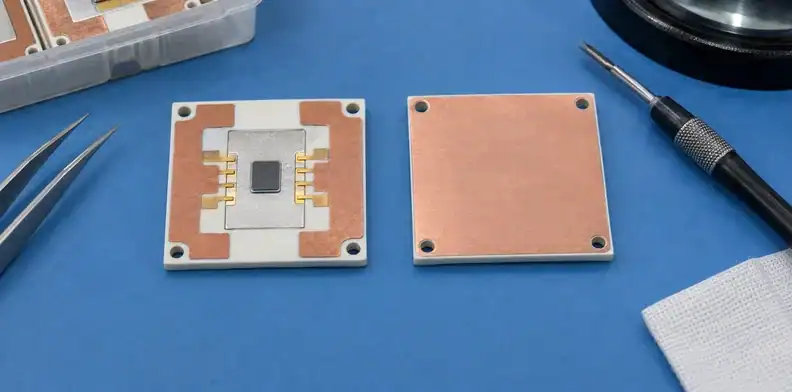
The cooler-facing surface
Describe the back face by its actual connection. A substrate sintered to a baseplate presents a metal-to-attach-material interface. A substrate pressed against a cooler through a thermal interface material presents a different contact arrangement, including its mounting condition. “Backside finish same as front” can conceal that difference.
For illustration, consider a frontside die-sintering design whose backside is mechanically mounted against a cooler. Frontside paste compatibility should not dictate a backside coating change without checking the cooler interface. Show the backside copper outline, coating coverage and mounting surface in a separate view so that an optional finish cannot migrate into that interface unnoticed.
Which surface can accept the specified bonding wire?
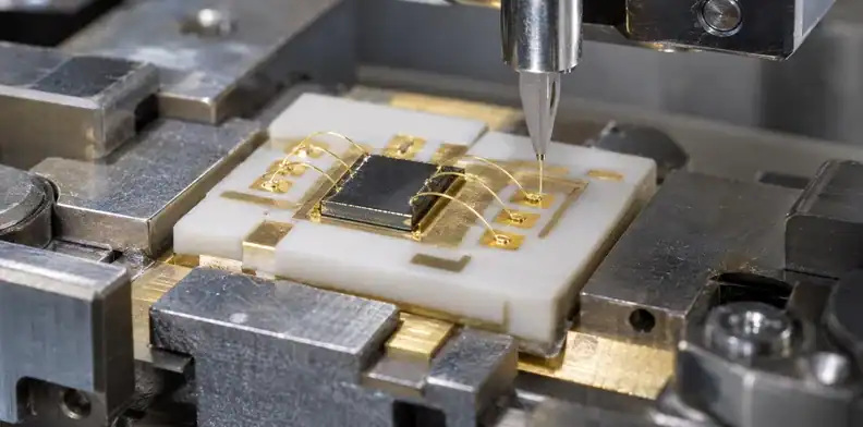
Select a wire-bond candidate by the wire alloy, bonding method and finished pad condition. ENEPIG and bondable gold systems are candidates for evaluation; their names alone do not qualify a ceramic assembly. Electroless nickel/electroless palladium/immersion gold (ENEPIG) identifies a layer sequence; the nominated wire-to-pad combination still needs qualification.
Gold wire on a qualified finish
Identify whether the drawing calls for gold ball bonding, wedge bonding or another process. The pad trial should use the chosen wire and tool, with the substrate supported as it will be in assembly. An advertised “wire-bondable” finish leaves these process conditions unspecified.
IPC-4556 addresses ENEPIG applications including soldering, wire bonding and contact finishes. Its public scope and contents establish the document’s subject; the project still needs the applicable purchased revision and assembler-approved requirements. Avoid lifting a thickness range from an unrelated website into a ceramic drawing.
| Proposed finish description | Clarification before a bonding trial | Assumption to avoid |
|---|---|---|
| ENEPIG | Actual Ni/Pd/Au stack and assembly history | Every deposited stack bonds identically |
| Bondable soft gold | Deposition route, underlayers and specified gold system | Any gold-colored coating is equivalent |
| ENIG | Exact gold deposition and evidence for the intended wire process | Ordinary soldering acceptance proves bondability |
| Copper or silver surface | Complete conductor and finish system accepted by the assembler | A die-sinter finish is automatically a wire-bond finish |
The ENIG, hard-gold and soft-gold discussion separates those finish purposes. Use it for background while keeping the ceramic order tied to its nominated wire process.
Aluminum wire and ribbon need their own trial
An aluminum wedge or ribbon process cannot be qualified by presenting a successful gold-wire coupon. Its wire material, landing footprint, tool and loading conditions are different inputs. Record those inputs even when both operations use a finish from the same family.
The ENEPIG and ENIG comparison covers their general soldering and bonding roles. For the ceramic assembly, require the bonding owner to accept the actual land surface and trial specimen. Keep wire-to-die and wire-to-substrate results identifiable, because they assess different surfaces within the same interconnect.
Select the silver paste before freezing the finish
Silver-sinter compatibility is specific to the paste, substrate surface and die backside metallization. Silver plating is one candidate, but published paste offerings also support selected gold or copper surfaces. Choose a material and process combination before specifying an alternative finish.
Heraeus lists Au, Ag and Cu for its PE338 pressure-sinter product, while its DA295 A pressureless product lists Au and Ag and is described as optimized for ENIG PCB surfaces. These are product-specific examples, not a common process window. The Heraeus sinter-material tables illustrate why “silver sintering requires only silver” and “ENIG can never be sintered” are both too broad.
| Published material example | Product’s stated surface scope | Project question left to resolve |
|---|---|---|
| Heraeus PE338 | Au, Ag and Cu; pressure sintering | Which surface-specific process and support arrangement applies? |
| Heraeus DA295 A | Au and Ag; pressureless; ENIG optimization stated | Does the offered stack and die size fit the selected application? |
| Dycotec DM-SSA-10302S | Copper, gold and silver; pressureless paste | Is the actual substrate/die pair accepted for this formulation? |
| ALPHA Argomax 2048 | Gold/silver finished substrates; pressure package attachment | Does the proposed application match its package-to-base attachment scope? |
The table lists published application scope. A fabrication specification needs project-approved deposits and boundaries. Dycotec’s particular paste page and MacDermid Alpha’s package-attach product provide the corresponding scope.
An RFQ should identify the die’s backside layer system as well as the ceramic’s top finish. Compatibility on one side of the joint leaves the other side unresolved. Request the paste manufacturer’s application guidance for that pair, including the deposition method, drying, atmosphere, temperature and any applied pressure.
When approaching a ceramic substrate fabrication supplier, state whether the paste is already selected or remains an engineering variable. Quote candidate surfaces as alternatives for evaluation when needed; do not approve them as interchangeable production substitutions.
Qualify bond lands after the preceding heat exposure
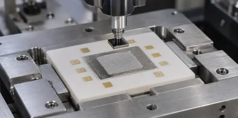
Test wire-bond lands in the condition they reach after die attachment and any earlier thermal operations. As-supplied plating measurements describe the starting substrate; they cannot establish the bonding response of a surface that has since been heated, cleaned or handled.
What a published wire-bond study demonstrates
An original study by Oda and colleagues at Uyemura varied palladium and gold deposits and evaluated wire bonding after a defined heat treatment. Their experiment used copper-clad laminate specimens and 1 mil gold wire, with a 175°C, 16-hour exposure before bonding. It examined pull results and fracture surfaces while changing the finish layers. The published paper relates bonding response to the deposited stack and thermal condition.
Use the study’s comparison method: evaluate the finish after a representative exposure and examine how the joint fails. The paper’s laminate specimens and selected process conditions do not qualify a ceramic substrate, aluminum ribbon or another gold deposition. Its measured values should not become the acceptance limit for a different construction.
Translate the method to a ceramic assembly
For an illustrative trial, split substrates from the same defined finish lot into as-supplied witnesses and witnesses taken through the planned die-attach sequence. Use the same nominated wire process for comparison, with individual results associated with the substrate face, land location and thermal-history record. This arrangement helps distinguish an initially unsuitable surface from a change introduced before bonding.
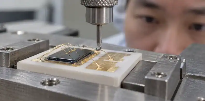
Record fracture location alongside strength. A break in the wire, separation at the finish or damage involving the conductor-to-ceramic interface lead to different investigations. A single average value can hide that information, so retain individual results and images of representative failures.
The assembler should set the sample plan and acceptance criteria for the intended product. Retest the affected surface after changing the cleaning or attach cycle, even if the original plating certificate is unchanged. No successful trial or lifetime result is implied by this proposed comparison.
How roughness and support change the interface
Specify surface topography at the functional location, and evaluate ceramic support with the attachment process. A general ceramic roughness value or a backside flatness result does not describe every die land and wire land on the finished part.
Measure the functional surface
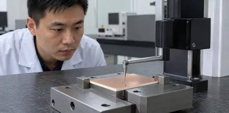
A roughness requirement needs a named parameter, method, measurement direction or area, and surface state. Ra and Rz are different descriptors; values reported for bare ceramic, circuit copper and deposited finish should remain distinguishable. Include a measurement location on the finish overlay so that a convenient open area cannot silently replace the critical land.
Rogers discusses different roughness needs for fine-wire bonding, thin sinter layers, cooler interfaces and molding. Evaluate each interface’s roughness requirement separately. A smooth surface selected for attachment should not automatically become the requirement for a region intended to adhere to encapsulant.
Keep local topography separate from whole-substrate shape. The ceramic warpage and attachment discussion addresses that broader geometry. Record the local finished surface contacted by the wire or paste.
Support the ceramic during attachment
A pressure-sinter proposal needs a sketch of the supported stack, including the load footprint, backside contact and any openings below the loaded area. Review the press tooling with the assembler before assuming a pressure setting published for a material can be applied to this substrate geometry.
For example, a fixture that supports one coupon fully can differ from a fixture used for a substrate with a backside recess. Treat that as a mechanical review question, not evidence that either arrangement will fail. Ask how the attachment force is transferred through the ceramic and which surfaces are intended to contact the fixture.
Verify the proposed arrangement on the representative construction. Changes to the underside geometry or support should remain visible in the trial record because the same paste and top finish can otherwise conceal a changed attachment condition.
Keep earlier assembly steps off the bond lands
Keep unbonded lands clear of attachment material and validate their condition after the preceding operations. The relevant sequence includes printing or dispensing, die placement, attachment, any cleaning and the interval before wire bonding.
Rogers notes that solder residues can affect subsequent wire bonding and discusses solder mask or copper grooves as containment options on its substrates. Containment needs evaluation for the chosen assembly; a groove, mask opening or selective-finish boundary should not be assumed to control every paste or solder process.
An illustrative process review can proceed through these specific questions:
- Does the deposited material stay within its intended die-attach region after placement?
- Are solder terminals joined before bonding, and which nearby lands are exposed to that operation?
- What cleaning method is approved for the finish and attachment material?
- Where are the substrates held between cleaning and bonding, and how are opened trays identified?
- Which inspection establishes that the bond lands remain available and undamaged?
Use the ceramic reflow-profile article for solder-temperature development when soldering is part of the sequence. Develop the silver-sinter cycle from the selected material’s process requirements.
Avoid writing “plasma clean before bonding” as a universal repair instruction. The assembler needs a qualified treatment for the particular surface and process history. Likewise, a shipping shelf-life statement does not specify the permitted exposure after a tray has been opened and substrates have passed through attachment.
Attach the agreed sequence and intermediate handling conditions to the trial traveler. That makes the tested surface condition repeatable when the ceramic moves from sample fabrication into assembly.
Write a finish drawing that CAM can quote
Give computer-aided manufacturing (CAM) a dimensioned finish overlay tied to the conductor artwork and mechanical drawing. Finish names belong beside the regions they control, with a layer sequence and a boundary requirement that the fabricator can assess.
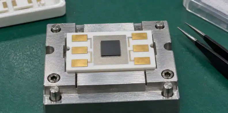
Provide front and back views with a shared origin and orientation. Identify the die land, wire lands, terminal areas, exposed ceramic and any fixture-contact restrictions. A colored preview can help discussion, but retain the dimensioned production file and its revision as the quoted reference.
An illustrative note for a mixed-function substrate could read:
Apply the approved silver finish only within die-attach region A. Apply the assembly-approved bondable stack to wire-land regions B. Backside region C follows the base-interface specification. Confirm deposited-layer requirements and selective-boundary tolerances against the accompanying finish drawing before fabrication.
This is a note structure, not a released coating specification. Replace the region letters with actual drawing definitions and fill in the approved materials, layer requirements and tolerances. An unspecified “approved stack” still leaves the quote incomplete.
Check how the plating boundary relates to the usable wire landing footprint and the attach-material footprint. A line drawn exactly on a die edge leaves no stated allowance for selective-processing variation or deposited-material spread. The designer and fabricator should agree the boundary using actual geometry and process capability.
Ask the fabricator to return a marked drawing if masking, electrical connections for plating or its proposed process change coverage. Resolve those marked differences before ordering the trial substrates. A revised finish overlay can affect the assembly interfaces even when the circuit artwork is unchanged.
Separate plating measurements from assembly validation
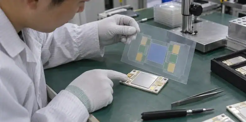
Use finish measurements to confirm deposited layers and assembly tests to assess the resulting joints. These reports answer different questions; one cannot replace the other simply because both mention gold, silver or ENEPIG.
X-ray fluorescence (XRF) can analyze coating composition and thickness through a defined layer model. Bruker’s micro-XRF coating analysis resource describes point measurements, distribution maps and calibration comparisons. For a selective ceramic finish, identify the measured region and the model used for that metal stack.
| Evidence item | What it can support | What remains unproven |
|---|---|---|
| Layer-thickness report | Deposits at the reported locations and conditions | Wire or sinter-joint performance |
| Finish coverage inspection | Boundaries and visible surface condition | All contamination or subsurface defects |
| Bond pull or suitable shear trial | The tested wire/pad process and failure behavior | A different wire alloy or untested heat history |
| Die-attach mechanical trial | The tested die, finish, paste and joint condition | Every die size or another attach recipe |
| Qualification exposure plus interface examination | Behavior of the tested assembled construction | Lifetime of a different module or operating profile |
Use the finish-thickness evidence discussion for general measurement-report questions. The ceramic-specific addition is to connect each measurement to the front/back zone and each joint test to its actual assembly history.
For destructive attachment tests, request the specimen geometry, test method, loading condition and fracture description alongside the result. If an inspection method is proposed to find interface defects, establish which interface it can resolve on the actual stack before making it an acceptance requirement.
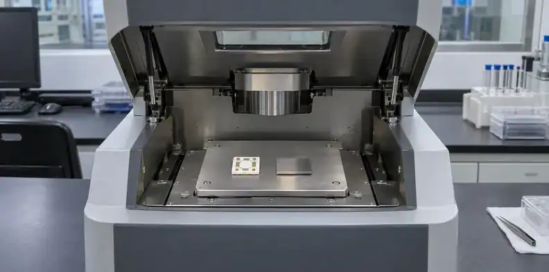
Agree separately what the substrate shipment includes and what the assembler’s trial report includes. The receiving team can then check finish identity and promised measurements, while the assembly owner evaluates bonding and attach results against the product’s defined criteria.
Send a ceramic interface package for quotation
A useful ceramic quotation identifies the fabricated surfaces and the assembly work being requested. Separate bare-substrate supply, assembled trial specimens and any qualification testing so that suppliers quote the same deliverable.
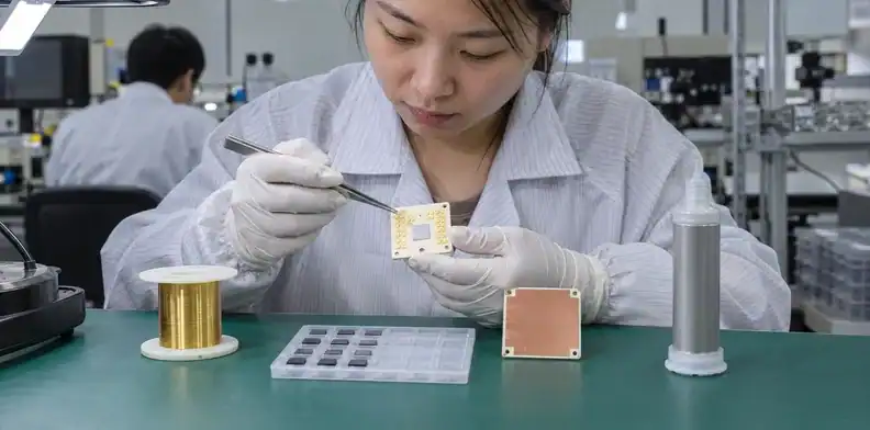
Send the ceramic construction drawing, conductor files, front/back finish overlay and proposed finish-layer requirements together. Add the bonding wire designation, diameter and method; die dimensions and backside metallization; selected sinter material; and the intended attachment sequence. Mark variables that still require a trial as provisional.
List substrate quantities separately from quantities consumed by destructive testing. Specify which finish regions need measurement reports and which assembled interfaces need trial records. An order for bare ceramics should not silently assume that die shear or wire pull testing is included.
Keep the assembly owner involved when a supplier proposes an alternate stack or selective-plating route. Include the technical difference, required trial specimens and test scope in the commercial comparison. Once a combination is accepted, preserve the finish overlay and assembly-material identifiers for the next lot.
Send these interface drawings, wire details, die-backside data, paste designation and trial quantities through the QueenEMS ceramic project inquiry. Ask the quotation to identify the offered substrate construction, surface assumptions and separately scoped assembly or validation work.
Sources
Written by the QueenEMS Engineering Team
Upload your files today · Free DFM check before production · Ship worldwide
Get your PCB prototypes in as fast as 24 hours. We handle FR4, Rogers, and hybrid boards up to 40 layers in volume production, with advanced builds subject to engineering review — free prototypes for 2–4 layer FR-4 boards, no minimum order.
Just upload your Gerber + BOM — we source every part, assemble, and inspect (AOI + X‑Ray) so you don't have to chase suppliers. Boards ship in as fast as 24 hours.