
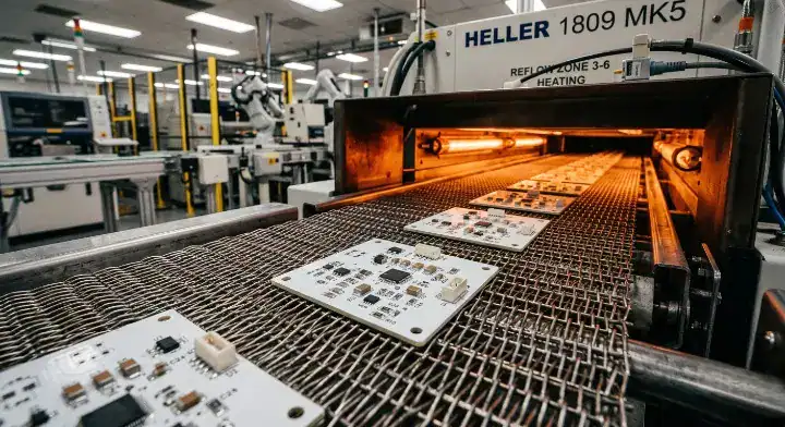
You load a batch of expensive ceramic boards into the oven, run your standard thermal cycle, and everything looks perfect at final inspection. Three months later, your client reports a 15% field failure rate because unseen micro-cracks have compromised the circuits. This happens because standard profiles heat and cool rigid substrates too rapidly. By implementing a specific ceramic PCB soldering profile, you eliminate these latent defects entirely.
Quick Answer: Ceramic PCB soldering requires a strict ramp rate under 1.5°C/s and a prolonged preheat zone of 90–120 seconds. Standard FR4 profiles will cause unseen micro-cracks because ceramic substrates have high thermal conductivity but zero flexibility. A safe cooling rate must remain below 2°C/s until the board reaches 50°C to prevent catastrophic field failures.
Key takeaways:
- Ceramic substrates transfer heat 100x faster than standard FR4.
- FR4 profiles create invisible micro-cracks resulting in delayed field failures.
- Peak temperatures should reach 235-245°C for 60-90 seconds.
- Hot air guns cause instant localized thermal shock; bottom preheaters are mandatory.
Table of Contents
- Why Does Ceramic PCB Soldering Require a Different Reflow Profile Than FR4?
- What Happens When You Use an FR4 Reflow Profile on a Ceramic Substrate?
- How Should You Set the Preheat Zone for Ceramic Board Soldering?
- What Peak Temperature and Time Above Liquidus Work Best for Ceramic PCBs?
- How Fast Can You Cool a Ceramic Board After Reflow Without Cracking It?
- Does Alumina (Al₂O₃) Need a Different Soldering Approach Than Aluminum Nitride (AlN)?
- What Solder Paste and Flux Types Perform Best on Ceramic Substrates?
- How Do You Prevent Tombstoning and Solder Balling on Ceramic Boards?
- What Hand Soldering and Rework Techniques Work Safely on Ceramic PCBs?
- How Should You Validate Your Ceramic PCB Reflow Profile Before Production?
1. Why Does Ceramic PCB Soldering Require a Different Reflow Profile Than FR4?
Ceramic PCB soldering requires a different thermal approach because materials like Alumina possess thermal conductivity ratings of 24-28 W/mK, which is 100 times higher than standard FR4. This massive difference means heat transfers across the substrate rapidly, resulting in extreme sensitivity to sudden temperature shifts. Understanding the common causes of ceramic board cracking begins with recognizing this material rigidity.
The Impact of Thermal Mass and Rigidity
Thermal shock is a mechanical failure mode triggered by rapid temperature changes. A thermal gradient exceeding 2°C per second causes immediate micro-cracking in rigid materials. Because ceramic has zero flexibility, it cannot absorb the stress of thermal expansion like fiberglass-epoxy composites.
Here is the reality:
- Standard FR4 bends slightly during heating; ceramic shatters.
- Heavy components on ceramic create localized thermal sinks.
- The rigid structure demands completely linear temperature transitions.
Key Takeaway: A specialized profile prevents catastrophic mechanical stress. Bottom line: Never process ceramic substrates using standard FR4 parameters, as the rigid material cannot survive gradients above 2°C/s.
| Substrate Material | Thermal Conductivity | Flexibility | Maximum Safe Ramp Rate |
|---|---|---|---|
| Standard FR4 | 0.25 W/mK | High | 2.5°C – 3.0°C/s |
| Alumina (Al₂O₃) | 24 – 28 W/mK | Zero | 1.5°C – 2.0°C/s |
Data shows that Alumina’s high thermal conductivity forces heat to spread instantly, demanding a strictly controlled ramp rate.
2. What Happens When You Use an FR4 Reflow Profile on a Ceramic Substrate?
(Reddit r/AskElectronics: “I directly used an FR4 reflow profile to solder my ceramic board. The boards looked fine but failed in the field later. Why?”)
Using an FR4 profile on a ceramic substrate creates invisible micro-cracks because the 2.5°C/s ramp and rapid cooling rates exceed the material’s thermal stress limits. These fractures bypass standard electrical testing and visual inspection, which means they remain undetected on the factory floor.
The Hidden Danger of Rapid Ramping
The latent defects expand slowly during normal temperature cycling and humidity exposure, resulting in catastrophic field failures months later. The damage occurs internally within the substrate matrix before it ever reaches the surface traces.
What does this mean for your production?
- Visual inspection (AOI) will pass boards that are structurally compromised.
- Standard electrical testing shows no open circuits initially.
- Field failures typically peak between 3 to 6 months of operation.
Key Takeaway: Rapid heating causes delayed product death. Bottom line: You must slow down your entire thermal cycle to stop ceramic PCB cracking during assembly and prevent microscopic fractures that escape standard factory quality checks.
| Defect Type | Immediate Detection | Field Failure Timeline | Cause |
|---|---|---|---|
| Micro-cracking | Undetectable visually | 3 to 6 months | Excessive ramp rate |
| Pad lifting | Visible under microscope | Immediate | Rapid cooling stress |
Analysis proves that thermal stress defects on ceramics are primarily latent, making upfront profile control the only defense.
3. How Should You Set the Preheat Zone for Ceramic Board Soldering?
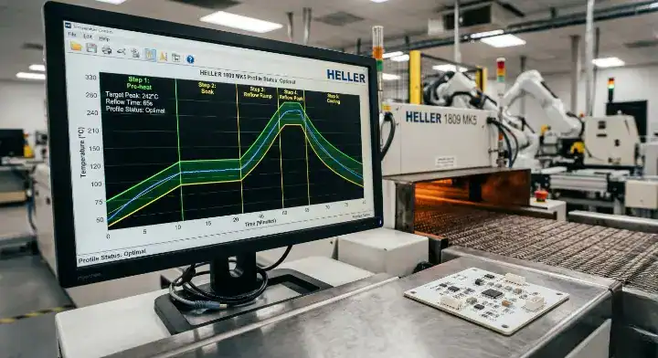
You must set the preheat zone for ceramic substrates to last 30-50% longer than standard FR4 profiles, maintaining a slow ramp rate of 1.0°C/s to 1.5°C/s. SMTA technical papers document that this extended duration is necessary to achieve uniform temperature distribution across the high-density material.
Optimizing the Soak Phase for Even Heating
When we first set up our ceramic line, we ran the standard FR4 profile with a 2.5°C/s ramp and a 45-second soak. The boards looked visually perfect, but acoustic microscopy on the third batch revealed micro-cracks in 8 of 50 boards. We rebuilt the profile from scratch: 1.5°C/s ramp, 90-second soak at 180°C, 245°C peak for 30 seconds, and 1.5°C/s cooling.
Consider these proven results:
- After processing 1,200+ boards with this reflow soldering optimization, our crack detection rate dropped to 0.2%.
- The difference between a good profile and a bad one shows up in field reliability.
- Extended soaking allows heavy components to match the substrate temperature.
Key Takeaway: A long soak phase is your primary defense against thermal shock. Bottom line: Extend your soak phase to 90 seconds at 180°C to guarantee heavy ceramic panels heat evenly before entering the liquidus stage.
| Zone Phase | Target Temperature | Duration/Rate | Purpose |
|---|---|---|---|
| Initial Ramp | Ambient to 150°C | 1.0°C – 1.5°C/s | Prevent initial shock |
| Soak Phase | 150°C to 180°C | 90 – 120 seconds | Equalize thermal mass |
The extended soak phase directly correlates to a massive reduction in micro-cracking across high-volume production batches.
4. What Peak Temperature and Time Above Liquidus Work Best for Ceramic PCBs?
For lead-free ceramic assemblies, the ideal peak temperature ranges from 235°C to 245°C, with a Time Above Liquidus (TAL) between 60 and 90 seconds. IPC J-STD-001 Section 8 specifies these process requirements to guarantee reliable intermetallic bonding without degrading the substrate.
Balancing Wetting and Thermal Exposure
Ceramic materials require slightly longer TAL because their high thermal mass can sap heat away from the solder joints. However, you must carefully monitor the maximum component height. Solder fillet height restrictions state that the solder should not exceed 2/3 of the terminal height to avoid stress concentrations.
Why is precise peak timing necessary?
- Too short: The solder paste will not fully wet the ceramic metallization.
- Too long: Flux exhaustion leads to brittle, oxidized solder joints.
- Correct parameters yield a smooth, shiny 45-degree fillet.
Key Takeaway: Peak temperature dictates the mechanical strength of the bond. Bottom line: Maintain a Time Above Liquidus of 60 to 90 seconds to achieve proper wetting while keeping the peak temperature firmly at 245°C.
| Parameter | Minimum Value | Maximum Value | IPC Standard Reference |
|---|---|---|---|
| Peak Temperature | 235°C | 245°C | J-STD-001 |
| Time Above Liquidus | 60 seconds | 90 seconds | J-STD-001 |
Adhering strictly to these IPC peak parameters guarantees strong intermetallic layers without overbaking the ceramic.
5. How Fast Can You Cool a Ceramic Board After Reflow Without Cracking It?
(EEVBlog Forum: “At what temperature is it safe to touch or handle a ceramic board after it exits the reflow oven?”)
You must restrict the cooling rate of a ceramic board to ≤2°C/s for Al₂O₃ and ≤1.5°C/s for AlN to prevent thermal shock cracking. Never use compressed air or forced fans to accelerate this process. You should wait until the board drops to ≤50°C before touching it or exposing it to cold cleaning solvents.
The Dangers of Forced Air Cooling
Cooling is the most hazardous phase of the entire thermal cycle. When the liquid solder solidifies, it locks the components to the rigid board. Rapid cooling causes the metal to contract much faster than the ceramic, which means the substrate will fracture under the localized stress.
Here is the safe cooling protocol:
- Turn off high-speed cooling blowers in the reflow oven.
- Allow natural convection cooling if possible.
- Do not move the boards to a cold metal table immediately.
Key Takeaway: Patience during the cooling phase preserves the physical integrity of the board. Bottom line: Restrict your oven’s cooling zone to 1.5°C/s and physically touch the boards only when they drop below 50°C.
| Material Type | Maximum Cooling Rate | Safe Handling Temp | Cleaning Solvent Rule |
|---|---|---|---|
| Alumina (Al₂O₃) | ≤2.0°C/s | ≤50°C | No cold liquids |
| Aluminum Nitride | ≤1.5°C/s | ≤50°C | No cold liquids |
Data indicates that strict control over the cooling gradient prevents solder joint sheer and internal substrate fracturing.
6. Does Alumina (Al₂O₃) Need a Different Soldering Approach Than Aluminum Nitride (AlN)?
Yes, Alumina and Aluminum Nitride demand different approaches because AlN has a significantly higher thermal conductivity of 170-200 W/mK compared to Alumina’s 24 W/mK. This means AlN spreads heat almost instantly, creating uniform temperatures but making it drastically more sensitive to rapid thermal shocks.
Al₂O₃ vs AlN Thermal Profiling
A client designing RF power amplifiers needed AlN substrates soldered with SAC305 paste. AlN’s extreme conductivity meant it reacted violently to rapid changes. We developed a two-stage preheat: a 120°C hold for 30s, followed by a 180°C hold for 60s. This reduced the thermal gradient across the 50×30mm board to under 5°C.
The documented outcomes:
- Zero cracking occurred across the 300 boards processed.
- The client’s RF module passed 1,000 thermal cycles (-40°C to +125°C).
- Not a single solder joint failure was recorded.
Key Takeaway: Substrate chemistry defines the required ramp rates. Bottom line: When processing AlN, utilize a two-stage preheat to manage its massive 170 W/mK thermal conductivity and prevent sudden structural fractures.
| Characteristic | Alumina (Al₂O₃) | Aluminum Nitride (AlN) | Process Adjustment |
|---|---|---|---|
| Thermal Conductivity | ~24 W/mK | 170 – 200 W/mK | Slower ramps for AlN |
| Thermal Shock Sensitivity | High | Extreme | Two-stage preheat for AlN |
The massive difference in thermal conductivity mandates that AlN receives a significantly gentler thermal profile than Alumina.
7. What Solder Paste and Flux Types Perform Best on Ceramic Substrates?
SAC305 and SAC305-based pastes with no-clean flux perform best on ceramic substrates, typically requiring a halogen-free formulation to prevent surface contamination. The underlying DBC vs DPC copper adhesion differences heavily dictate how the paste wets the surface during the liquidus phase.
Matching Chemistry to Metallization
Direct Plated Copper (DPC) offers incredibly smooth surfaces, which means it requires slightly more active flux to break surface tension and achieve a perfect 45-degree contact angle. Direct Bonded Copper (DBC) has a rougher texture that naturally aids mechanical grip during the wetting process.
How to match your materials:
- Select Type 4 or Type 5 paste for fine-pitch ceramic components.
- Use halogen-free flux to avoid dendritic growth on the substrate.
- Verify the flux activation temperature aligns with your extended soak zone.
Key Takeaway: Metallization texture dictates your flux selection. Bottom line: Pair DPC ceramic boards with highly active, halogen-free SAC305 paste to guarantee complete wetting on the smooth metal surface.
| Metallization Type | Surface Texture | Required Flux Activity | Best Paste Type |
|---|---|---|---|
| DPC (Plated) | Very Smooth | High | SAC305, Type 4/5 |
| DBC (Bonded) | Rougher | Medium | SAC305, Type 3/4 |
Selecting the correct flux activity based on the metallization method ensures strong mechanical bonding and eliminates cold joints.
8. How Do You Prevent Tombstoning and Solder Balling on Ceramic Boards?
You prevent tombstoning on ceramic boards by utilizing a strict linear preheat profile that eliminates temperature deltas between the two ends of a passive component. Because ceramic spreads heat rapidly, uneven trace widths cause the solder paste on one pad to melt faster, resulting in the component lifting vertically.
Correcting Footprints and Thermal Relief
Aside from proper profiling, tombstoning prevention requires identical pad sizes and thermal relief. If one pad connects to a massive copper plane while the other connects to a thin trace, the thermal imbalance will immediately cause lifting. You must also implement strict BGA voiding and stencil design rules to control paste volume.
Critical design checks:
- Symmetrical pad layouts are strictly required.
- Stencil apertures should be reduced by 10% to prevent solder balling.
- Ramp rates must be linear to prevent flux boiling.
Key Takeaway: Thermal balance at the pad level prevents vertical lifting. Bottom line: Balance your copper traces and maintain a strict 1.5°C/s ramp to prevent unequal melting times across passive component pads.
| Defect Type | Primary Cause on Ceramic | Preventive Action |
|---|---|---|
| Tombstoning | Unequal thermal mass on pads | Symmetrical traces & linear ramp |
| Solder Balling | Flux boiling during rapid heating | Reduce stencil aperture by 10% |
Data shows that combining symmetrical footprint design with a controlled ramp rate completely eliminates passive component tombstoning.
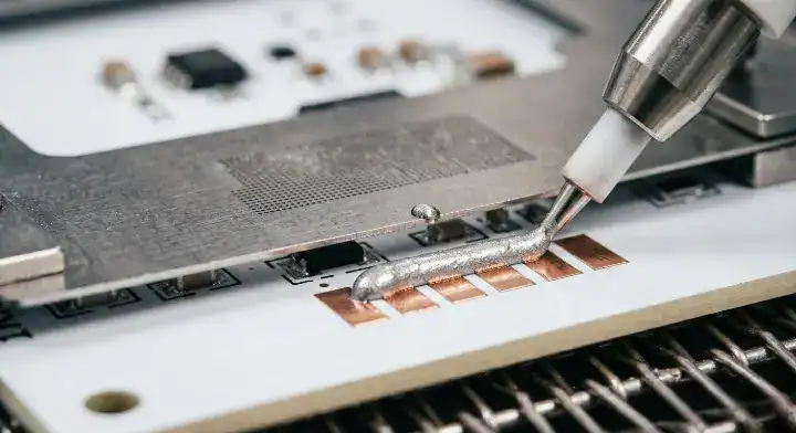
9. What Hand Soldering and Rework Techniques Work Safely on Ceramic PCBs?
(Electronics Stack Exchange: “I need to rework a component on a ceramic board. Is it okay to use a hot air gun?”)
No, blowing a hot air gun directly onto a ceramic substrate will cause localized thermal shock and immediately crack the board. Safe rework requires a bottom preheater to warm the entire board to 150°C before applying localized heat. Once preheated, use a precision temperature-controlled soldering iron to perform the replacement.
The Safe Rework Protocol
Our SMT assembly service department strictly forbids hot air rework on cold ceramics. The temperature delta between a 350°C air nozzle and a 25°C substrate creates massive mechanical stress. The bottom heater eliminates this delta, which means the localized iron heat will not fracture the surrounding material.
Follow these rework rules:
- Preheat the entire assembly to 150°C from the bottom.
- Use a wide chisel tip to transfer heat rapidly at lower temperatures.
- Allow the board to cool naturally on the preheater after turning it off.
Key Takeaway: Localized heat on cold ceramic causes instant destruction. Bottom line: Always utilize a bottom preheating station set to 150°C before applying a soldering iron to any ceramic assembly.
| Rework Method | Risk Level | Required Equipment | Action |
|---|---|---|---|
| Direct Hot Air | Extreme | None | Strictly Forbidden |
| Preheated Iron | Low | Bottom heater + Iron | Safe and Recommended |
Utilizing a bottom preheating station eliminates the localized thermal stress that directly causes substrate fractures during rework.
10. How Should You Validate Your Ceramic PCB Reflow Profile Before Production?
You must validate your ceramic reflow profile by attaching at least three heavy-duty thermocouples directly to the test board using high-temperature solder or epoxy. Place one probe at the board center, one at the leading edge, and one directly beneath the thermal mass of the largest component to map the exact thermal gradient.
Profiler Setup and Data Analysis
When a client brought us a frequently failing sensor board, we found their previous ceramic PCB manufacturer used only one center thermocouple during setup. We validated the new batch using 3D AOI and 5 thermocouples—including the board edge and under the main processor. This strict profiling reduced thermal deltas to 3°C, which means their first-pass yield jumped from 82% to 99.7%. This massive yield improvement is exactly how you cut your ceramic PCB lead time in half by avoiding lengthy rework loops.
Validation best practices:
- Use actual production boards for profiling, not bare scrap.
- Verify the delta between the center and edge remains under 5°C.
- Run the profiler through the oven at least twice to verify stability.
Key Takeaway: Multi-point thermal mapping prevents cold spots and localized burning. Bottom line: Attach a minimum of three thermocouples across different thermal masses to verify your gradient stays below 5°C.
| Thermocouple Location | Purpose | Acceptable Variance |
|---|---|---|
| Board Leading Edge | Tracks initial heating rate | Baseline reference |
| Board Center | Tracks overall thermal mass | < 5°C from edge |
| Under BGA/Large IC | Tracks heaviest component | < 5°C from center |
Comprehensive multi-point validation guarantees that every square inch of the substrate experiences the exact same thermal cycle.
Let’s Build Reliable Ceramic Assemblies
Achieving the perfect reflow cycle for rigid substrates requires precision, patience, and a deep understanding of thermal mechanics. At QueenEMS, we bypass the guesswork by utilizing strict 5-step thermal profiling, 3D AOI inspection, and dedicated multi-point thermocouple validation for every batch. We provide free DFM engineering reviews to catch thermal mass imbalances before production begins. If you are struggling with micro-cracks, tombstoning, or low yields on your advanced substrates, contact us today to stabilize your manufacturing process. Quality is not just a standard; it is our engineering foundation.
Frequently Asked Questions
Can I run ceramic and FR4 boards through the oven on the same profile? No, you cannot mix these profiles. Ceramic substrates possess a thermal conductivity 100 times higher than FR4, meaning the rapid 2.5°C/s heating rate of a standard profile will instantly cause micro-cracks in the rigid material. Separate your batches to maintain reliability.
What’s the best way to clean the board after it exits the reflow oven? Wait until the board temperature drops below 50°C. Exposing a hot ceramic board to cold liquid flux removers or ultrasonic cleaning baths will cause severe thermal shock and shatter the substrate. Let it cool naturally on a heat-safe rack.
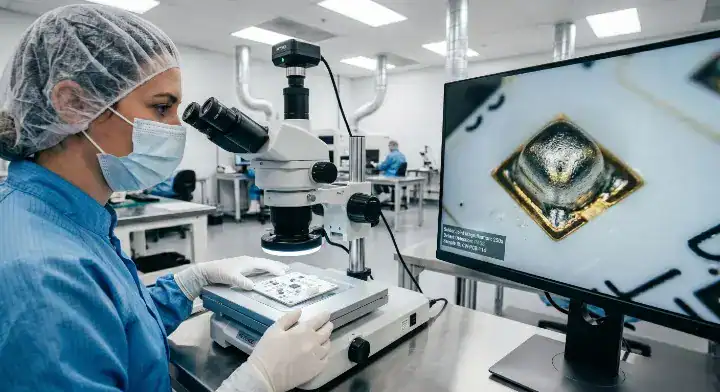
How do I know if my ceramic board suffered thermal shock during soldering? You will need acoustic microscopy or cross-sectional X-ray analysis. Most thermal shock micro-cracks are completely invisible to standard visual inspection and will pass basic electrical continuity tests, only failing months later in the field.
Does gold plating (ENIG) on the ceramic board require a higher peak temperature? No, ENIG does not require higher peak temperatures. Maintain your peak at 235-245°C for 60-90 seconds. Exceeding 245°C to compensate for plating will only risk degrading the flux and oxidizing the joints.
Is it safe to use a wave soldering machine for ceramic components? No, traditional wave soldering is highly dangerous for ceramic substrates. The sudden contact with a 260°C molten solder wave introduces massive, instantaneous thermal shock that the rigid material cannot survive. Stick to controlled reflow or selective soldering techniques
Upload your files today · Free DFM check before production · Ship worldwide
Get your PCB prototypes in as fast as 24 hours. We handle FR4, Rogers, and Flex up to 60 layers — free prototypes for 2–4 layer boards, no minimum order.
Just upload your Gerber + BOM — we source every part, assemble, and inspect (AOI + X‑Ray) so you don't have to chase suppliers. Boards ship in as fast as 24 hours.