
Quick Answer: The ceramic PCB manufacturing process utilizes 7 core technologies (DBC, DPC, AMB, thick film, thin film, LTCC, and HTCC) to bond conductive copper to inorganic substrates. DPC achieves ultra-fine 50μm trace resolutions, DBC handles extreme copper thicknesses up to 800μm, and tooling costs range from $150 for thick film to $5,000+ for complex HTCC multi-layer designs.
Key takeaways:
- DBC forms a Cu-O eutectic bond at 1065–1085°C, delivering high peel strength (>1.4 N/mm) for heavy copper applications.
- DPC uses vacuum sputtering and electroplating at 250–350°C, providing the tightest 50/50μm trace/space resolution.
- LTCC adds 30–50% glass frit to lower firing temperatures, which drastically reduces thermal conductivity to 2–3 W/m·K.
- AMB brazes active metals like Titanium in a vacuum at 700–900°C, offering superior thermal cycling reliability for automotive EV modules.
Table of Contents
- What Are the 7 Technologies in the Ceramic PCB Manufacturing Process?
- How Does the Direct Bonded Copper (DBC) Process Work?
- Why is Direct Plated Copper (DPC) Replacing DBC in Many Designs?
- When Should You Choose Active Metal Brazing (AMB) for Ceramic PCBs?
- What Are the Differences Between Thick Film and Thin Film Ceramic PCB Fabrication?
- How Do LTCC and HTCC Ceramic Substrate Manufacturing Processes Compare?
- DBC vs DPC vs AMB: Which Post-Fired Technology Wins?
- How to Choose the Right Ceramic PCB Manufacturing Process for Your Design?
- What Are the Key Design for Manufacturing (DFM) Tips for Each Process?
- How Does the Ceramic PCB Manufacturing Process Impact Your Final Cost?
The ceramic PCB manufacturing process determines the maximum heat dissipation, trace resolution, and mechanical reliability of your electronic module. You are designing a high-power device and need superior thermal management, but choosing the wrong fabrication method leads to catastrophic field failures or ruined budgets. We constantly see engineers overpay for HTCC boards when a simple DPC substrate would solve their thermal issues perfectly. By understanding the specific limits of all 7 commercial manufacturing technologies, you can match your board to the most cost-effective production method available.
What Are the 7 Technologies in the Ceramic PCB Manufacturing Process?
The ceramic PCB manufacturing process consists of 7 commercial technologies that handle copper thicknesses from 10μm to 800μm. These distinct methods dictate how the conductive metal bonds to the ceramic base, requiring factory firing temperatures that span from 250°C up to 1700°C depending on the chosen chemistry.
Categorizing the Fabrication Methods
Here is the reality: you must categorize these technologies to understand their applications. Post-fired ceramics (DBC, DPC, AMB) bond metal to pre-hardened substrates. Co-fired ceramics (LTCC, HTCC) bake the conductive paste and green ceramic tape simultaneously.
- Post-fired methods yield the highest thermal conductivity.
- Co-fired methods allow for extreme multi-layer stacking (10+ layers).
- Film methods (Thick/Thin film) deposit metal onto bare substrates for cost-effective or ultra-precise circuits.
Understanding the Capability Range
To select the right technology, you need to align your design’s physical demands with the process capabilities. The choice between these 7 methods completely changes your routing density.
Key Takeaway
Bottom line: Group your design requirements by layer count and thermal density first; use post-fired methods for 1-4 layer high-power designs, and co-fired methods for 10+ layer RF or high-density routing.
| Process Category | Specific Technologies | Primary Advantage | Typical Layer Count |
|---|---|---|---|
| Post-Fired | DBC, DPC, AMB | Highest thermal conductivity (24-230 W/m·K) | 1-4 layers |
| Co-Fired | LTCC, HTCC | High-density 3D routing | 10-40+ layers |
| Film Deposition | Thick Film, Thin Film | Cost efficiency or extreme RF precision | 1-2 layers |
Analyze your layer count requirements before specifying a process, as post-fired methods become cost-prohibitive beyond 4 layers.
How Does the Direct Bonded Copper (DBC) Process Work?
The Direct Bonded Copper (DBC) ceramic PCB manufacturing process bonds copper foil to a ceramic base by heating them to 1065–1085°C to form a Cu-O eutectic liquid. This method supports massive copper thicknesses between 150μm and 800μm, achieving an incredible peel strength greater than 1.4 N/mm.
The DBC Bonding Mechanism
DBC is a high-temperature bonding technique. The factory introduces a controlled amount of oxygen between the copper and ceramic inside a high-temperature nitrogen furnace. At 1065°C, the copper and oxygen react to form a thin eutectic fluid that aggressively wets both the ceramic surface and the solid copper foil, creating a permanent molecular bond when cooled.
Resolution Limitations
What does this mean for you? Because DBC relies on thick copper foils and heavy chemical etching, its resolution capabilities are severely limited.
- The minimum line and space resolution sits between 150μm and 300μm.
- Chemical etching causes aggressive undercutting on thick copper layers.
- DBC cannot support plated through-holes (PTH) easily.
Key Takeaway
Bottom line: Specify DBC exclusively for high-current industrial controls and power modules where you need massive copper thickness (>150μm) and do not require fine-pitch routing.
| DBC Parameter | Capability Specification |
|---|---|
| Bonding Temperature | 1065°C – 1085°C |
| Copper Thickness | 150μm – 800μm |
| Min Trace/Space | 150μm / 150μm (Coarse) |
| Peel Strength | > 1.4 N/mm |
Avoid DBC if your design includes micro-controllers or fine-pitch BGAs, as the 150μm minimum trace width will cause severe routing failures.
Why is Direct Plated Copper (DPC) Replacing DBC in Many Designs?
Direct Plated Copper (DPC) uses vacuum sputtering followed by electroplating at 250–350°C, achieving ultra-fine 50/50μm trace and space resolutions. Engineers are replacing DBC with DPC because modern electronics require microscopic routing capabilities that DBC’s heavy etching process simply cannot deliver.
Overcoming DBC Resolution Limits
Engineers face a common dilemma: they want ceramic thermal performance but need high-density routing. DPC solves this. Vacuum sputtering deposits an ultra-thin titanium/copper seed layer directly onto the ceramic. We then use standard semi-additive photo-lithography and electroplating to build the copper traces up to 10–300μm thick.
Think about it this way: DPC brings the precision of standard FR-4 fabrication to ceramic substrates.
Real Factory Application
A client attempted to use a DBC board for a medical sensor requiring 50μm traces, resulting in a 100% failure rate due to severe acid etching undercut. At QueenEMS, we ran a free DFM review and transitioned their design to a vacuum-sputtered DPC process. Because DPC uses additive plating instead of subtractive etching, we achieved a 99.7% first-pass yield rate with perfect 50μm trace geometry.
Key Takeaway
Bottom line: Choose the DPC process when your ceramic design requires fine lines under 100μm, plated through-holes, or precision BGA mounting.
| Process | Core Mechanism | Min Resolution | Copper Range |
|---|---|---|---|
| DBC | Cu-O Eutectic Firing | 150μm / 150μm | 150 – 800μm |
| DPC | Vacuum Sputtering + Plating | 50μm / 50μm | 10 – 300μm |
Select DPC for microelectronics and LEDs requiring fine-pitch components, and reserve DBC for brute-force power transmission.
When Should You Choose Active Metal Brazing (AMB) for Ceramic PCBs?
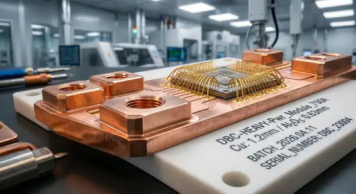
The AMB ceramic PCB manufacturing process brazes active metals like Titanium between copper and ceramic in a vacuum at 700–900°C, handling thermal cycling from -55°C to +150°C for 1,000 cycles. You should upgrade to AMB exclusively for automotive EV modules or rail transit systems where extreme mechanical reliability justifies the highest cost premium.
The Thermal Cycling Superiority
AMB is an advanced bonding technique. Unlike DBC which relies on oxygen, AMB uses a brazing paste containing active elements (Ti, Zr, or Hf). This paste chemically reacts with the ceramic (especially Aluminum Nitride or Silicon Nitride) under a high vacuum. This creates a bond so strong that it practically eliminates substrate micro-fractures during violent temperature swings.
- AMB retains >95% solder joint strength after 1,000 thermal cycles.
- It supports heavy copper up to 800μm on extremely thin ceramic layers.
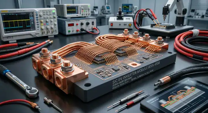
- It is the mandatory standard for Silicon Carbide (SiC) EV inverters.
Solving the EV Reliability Issue
An automotive client used standard DBC for an EV motor controller, but the substrate cracked after 500 thermal cycles during stress testing. We re-engineered the board using our AMB process with Titanium brazing on a Si3N4 substrate. The new AMB boards passed 1,000 extreme thermal cycles (-55°C to +150°C) with zero micro-fractures, securing their tier-1 automotive certification.
Key Takeaway
Bottom line: Do not pay the massive AMB premium for standard industrial devices; reserve it strictly for automotive, aerospace, or military applications facing extreme thermal shock and vibration.
| Reliability Metric | DBC Substrate | AMB Substrate |
|---|---|---|
| Thermal Cycling Limit | ~500 cycles | 1,000+ cycles |
| Temp Range Reliability | -40°C to +125°C | -55°C to +150°C |
| Ideal Ceramic Pairing | Al2O3 (Alumina) | Si3N4 (Silicon Nitride) |
| Cost Tier | Moderate | Very High |
Rely on AMB when your product warranty covers extreme environments where field replacements are impossible or dangerous.
What Are the Differences Between Thick Film and Thin Film Ceramic PCB Fabrication?
Thick film fabrication screen-prints conductive pastes and fires them at 850–900°C for low-cost sensors, while thin film relies on vacuum sputtering to achieve ultra-precise nanometer-level coatings. Thick film provides rapid, economical production for basic circuits, whereas thin film delivers extreme accuracy required for high-frequency RF and microwave applications.
The Thick Film Approach
Thick film technology is a mature printing method. Manufacturers use a stainless steel mesh screen to print pastes containing Silver (Ag), Gold (Au), or Silver-Palladium (Ag-Pd) onto the ceramic.
Here is the catch: the fired paste thickness is typically 10-25μm, and the resolution is relatively coarse (around 100μm). It is highly cost-effective and allows engineers to print integrated resistors directly onto the board.
The Thin Film Precision
Thin film technology is an ultra-precision deposition technique. Instead of printing, factories use magnetron sputtering or electron beam evaporation to deposit metals in a vacuum.
- Achieves trace widths down to 10μm.
- Provides exceptionally smooth metal surfaces.
- Drastically reduces signal loss at microwave frequencies.
Key Takeaway
Bottom line: Use thick film to mass-produce cheap automotive sensors and heaters, but mandate thin film fabrication for any RF telecommunications device operating above 10 GHz.
| Feature | Thick Film Process | Thin Film Process |
|---|---|---|
| Deposition Method | Screen Printing | Vacuum Sputtering |
| Typical Thickness | 10 – 25μm | < 1μm – 5μm |
| Line Resolution | ~100μm | 10μm |
| Primary Application | Sensors, Integrated Resistors | RF / Microwave circuits |
Evaluate your signal integrity requirements; if you are designing a standard analog sensor, thick film saves you massive setup costs.
How Do LTCC and HTCC Ceramic Substrate Manufacturing Processes Compare?
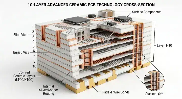
The LTCC ceramic PCB manufacturing process fires below 950°C by adding 30–50% glass frit, dropping thermal conductivity to 2–3 W/m·K, whereas HTCC fires at 1300–1700°C to achieve 20+ W/m·K. Both processes create high-density 3D structures by co-firing up to 40 layers of green ceramic tape, but they serve completely different technical needs.
The LTCC Glass Frit Bottleneck
Engineers frequently wonder why LTCC (Low-Temperature Co-Fired Ceramic) has such terrible heat dissipation compared to other ceramics. LTCC is a mixed composite. To lower the firing temperature from 1500°C down to 900°C, factories mix 30% to 50% glass frit into the ceramic slurry.
Because glass is a thermal insulator, this additive permanently destroys the pure ceramic thermal path, resulting in a thermal conductivity of just 2–3 W/m·K. This means LTCC is useless for high-power LED or IGBT heat management.
The HTCC Refractory Metal Requirement
HTCC (High-Temperature Co-Fired Ceramic) solves the thermal issue but creates a conductivity problem. Because HTCC fires at 1300–1700°C, you cannot use highly conductive metals like copper or silver (they would melt).
- HTCC requires refractory metals like Tungsten (W) or Molybdenum (Mo).
- These metals have poor electrical conductivity, increasing trace resistance.
- HTCC provides the highest mechanical strength and hermetic sealing capability.
Key Takeaway
Bottom line: Specify LTCC strictly for high-frequency RF modules requiring embedded passive components, and use HTCC for extreme aerospace environments requiring hermetic multi-layer packaging.
| Feature | LTCC (Low Temp) | HTCC (High Temp) |
|---|---|---|
| Firing Temperature | 800°C – 950°C | 1300°C – 1700°C |
| Conductor Metals | Ag, Au, Cu | W, Mo, Mn |
| Thermal Conductivity | 2 – 3 W/m·K | 20 – 24 W/m·K |
| Electrical Conductivity | Excellent | Poor |
Never select LTCC for power dissipation tasks; its thermal performance is barely better than standard FR-4 due to the glass additives.
DBC vs DPC vs AMB: Which Post-Fired Technology Wins?
DBC, DPC, and AMB dominate the post-fired market, but DPC wins for 50μm fine-pitch designs, DBC wins for raw 800μm current-carrying capacity, and AMB wins for -55°C to 150°C thermal cycling. Your choice depends entirely on whether you prioritize precise routing, brutal power loads, or extreme environmental survivability.
Direct Head-to-Head Comparison
The truth is, no single post-fired technology is universally superior. DBC remains the workhorse of industrial power electronics because of its cost-to-performance ratio. DPC owns the modern LED and micro-controller space due to its precise electroplating. AMB handles the rigorous demands of the electric vehicle transition.
Choosing incorrectly leads to either a burned-out trace (using DPC for too much current) or a cracked substrate (using DBC in an EV).
The Critical Decision Matrix
To simplify the factory quoting process, you must align your specs before submitting gerbers.
- If your trace width is <100μm, DBC is physically impossible.
- If your copper thickness must be 500μm, DPC is too slow and expensive.
- If your product goes into an automotive chassis, AMB is mandatory.
Key Takeaway
Bottom line: Map your maximum current load against your tightest trace pitch to instantly decide between DBC and DPC, keeping AMB as a backup solely for heavy vibration and thermal shock scenarios.
| Parameter | DBC (Direct Bonded) | DPC (Direct Plated) | AMB (Active Metal) |
|---|---|---|---|
| Best For | Heavy current, standard power | High density, fine pitch | EV, high reliability |
| Min Trace/Space | 150μm / 150μm | 50μm / 50μm | 200μm / 200μm |
| Max Copper | 800μm | 300μm (Practical) | 800μm+ |
| Relative Cost | Moderate ($$) | High ($$$) | Very High () |
Use this table during your initial design phase to prevent engineering a board that factories physically cannot manufacture.
How to Choose the Right Ceramic PCB Manufacturing Process for Your Design?
To choose the correct ceramic PCB manufacturing process, cross-reference your 5 core parameters: operating temperature, required copper thickness, minimum trace width, layer count, and cost sensitivity. A single hard constraint—such as needing 10 routing layers—instantly eliminates 5 of the 7 available technologies.
The 5-Parameter Selection Logic
Engineers get stuck because they view these processes as interchangeable. They are not. You must treat this as a rigid elimination game.
- Layer Count: Need >4 layers? You must use LTCC or HTCC.
- Minimum Trace Width: Need <50μm? You must use Thin Film or DPC.
- Copper Thickness: Need >400μm? You must use DBC or AMB.
- Operating Environment: Automotive extreme thermal shock? You must use AMB.
- Cost Sensitivity: Need mass-produced, cheap sensor arrays? You must use Thick film.
Navigating Competing Requirements
What does this mean for you? Sometimes your parameters conflict. If you need 10 layers (requiring LTCC/HTCC) AND excellent electrical conductivity (eliminating HTCC) AND good thermal dissipation (eliminating LTCC), you have an impossible design. You will need to break the design into a logic board (FR-4 or LTCC) and a separate power stage (DBC).
Key Takeaway
Bottom line: Lock in your layer count and trace resolution first to narrow your options, then select the cheapest remaining fabrication method that meets your thermal goals.
| Design Constraint | Recommended Process | Why? |
|---|---|---|
| >4 Routing Layers | LTCC / HTCC | Only co-fired methods support dense 3D stacking. |
| <50μm Fine Pitch | DPC / Thin Film | Additive plating/sputtering guarantees microscopic accuracy. |
| >400μm Heavy Copper | DBC / AMB | Strong eutectic/brazed bonds handle massive metal weight. |
| Lowest Cost (1-layer) | Thick Film | Screen printing is the fastest, cheapest high-volume method. |
Force your engineering team to fill out this parameter checklist before selecting a ceramic substrate material.
What Are the Key Design for Manufacturing (DFM) Tips for Each Process?
DFM rules dictate that DBC designs must avoid fine-pitch BGAs due to 150μm resolution limits, while HTCC designs must mathematically account for a 15–20% volumetric shrinkage during the 1500°C firing process. Failing to adjust your CAD files for the specific fabrication method guarantees a rejected batch at the factory level.
Designing for Shrinkage in Co-Fired Boards
Shrinkage is the biggest enemy in co-fired ceramics. Unlike post-fired methods where metal is applied to a hard substrate, LTCC and HTCC fire the soft “green tape” and metal together.
As the organic binders burn away, the entire board shrinks unpredictably by up to 20%. If your vias are not perfectly calculated, the layers will completely misalign.
Solving Registration Failures
A startup submitted a 12-layer HTCC design but failed to calculate the X-Y shrinkage ratio, which would have resulted in completely severed internal vias. Utilizing our full turnkey service, our QueenEMS engineers ran a free DFM/DFA engineering review. We mathematically scaled their pre-fire routing data by 16.5% to match our specific kiln profile, resulting in perfect layer registration and a successful 3D AOI inspection.
Key Takeaway
Bottom line: Never submit standard FR-4 design files for a ceramic order; you must request the factory’s specific design rules for trace spacing and shrinkage compensation beforehand.
| Process | Critical DFM Rule to Follow | Consequence of Failure |
|---|---|---|
| DBC | Maintain >150μm spacing. | Acid etch will destroy tight traces. |
| DPC | Use for plated through-holes (PTH). | DBC cannot easily plate through-holes. |
| LTCC/HTCC | Apply factory shrinkage ratio. | Total layer misalignment and via failure. |
| Thick Film | Limit to 1-2 layers. | Multi-layer printing causes severe unevenness. |
Partner with a manufacturer who runs automated DRC (Design Rule Checks) specifically calibrated for ceramic behavior before tooling begins.
How Does the Ceramic PCB Manufacturing Process Impact Your Final Cost?
The ceramic PCB manufacturing process creates massive cost tier variations, starting with Thick Film at $150 in tooling, scaling through DBC and DPC, and ending with HTCC which requires $5,000+ in custom molds and punch tools. You must select the lowest tier method that meets your thermal and electrical baseline to keep your product profitable.
Understanding the Cost Hierarchy
The cost of ceramic boards is not just about the raw Alumina or Aluminum Nitride substrate; it is heavily dictated by the factory tooling and setup time (NRE).
Here is the catch: Co-fired technologies (LTCC/HTCC) require custom mechanical punches for every single via on every single green tape layer. Post-fired technologies (DPC) use standard photolithography, making their setup costs much closer to standard rigid PCBs.
The Realistic Cost Tiers
To build an accurate budget, you must understand relative scaling. Assuming Alumina (Al2O3) is used as the base substrate for all compatible methods, the general cost progression from cheapest to most expensive is:
Thick Film < DBC < DPC < AMB < Thin Film < LTCC < HTCC
Key Takeaway
Bottom line: Start your design assuming standard DBC or DPC to minimize NRE costs, and only escalate to expensive AMB or HTCC tooling if your mechanical environment demands it.
| Process Tier | Relative Tooling Cost | Best For (Budget Perspective) |
|---|---|---|
| Thick Film | Very Low ($150 – $300) | Mass-market, low-margin analog sensors. |
| DBC / DPC | Moderate ($300 – $800) | Standard high-power LED and motor drives. |
| LTCC / HTCC | Extreme ($2000 – $5000+) | Aerospace and military defense budgets. |
Always calculate your expected production volume; the massive tooling cost of HTCC only pays off if you are ordering tens of thousands of units.
Every watt of heat and every micrometer of trace width dictates which manufacturing process your board requires. While HTCC and AMB offer bleeding-edge capabilities for extreme environments, standard DPC and DBC remain the undefeated champions of cost-effective power management.
At QueenEMS, we ensure your design matches the smartest manufacturing process. From our free DFM engineering reviews to 3D AOI + X-Ray inspection on every critical joint, we prevent costly fabrication mistakes before tooling even begins. With our up to 60-layer PCB fabrication capability and 24-hour fastest turnaround for rapid prototypes, we scale your project seamlessly from lab to mass production.
Stop guessing about your ceramic process selection. Contact us today for a data-driven process evaluation and an accurate tooling quote.
Written by the QueenEMS Engineering Team
FAQs
Can I use LTCC for a high-power 100W LED array? No, LTCC thermal conductivity drops to 2–3 W/m·K because the glass frit additives act as thermal insulators. You must use a post-fired process like DBC or DPC to maintain the pure ceramic 24+ W/m·K thermal path necessary for high-power LED cooling.
What’s the best process if I need 50μm traces on an Aluminum Nitride substrate? The Direct Plated Copper (DPC) process is the best choice. It uses vacuum sputtering and electroplating to achieve precise 50/50μm trace/space geometries, whereas DBC would destroy those fine lines during its aggressive chemical etching phase.
How do I know if my EV motor controller requires AMB instead of DBC? You need AMB if your thermal cycling requirements exceed 500 cycles at -55°C to +150°C. AMB uses active metal brazing (like Titanium) to create an incredibly resilient bond that resists micro-fracturing under extreme automotive temperature swings, unlike standard oxygen-bonded DBC.
Is the tooling cost for HTCC really that much higher than standard DPC? Yes, HTCC tooling costs easily exceed $2,000 to $5,000+ because the factory must create custom mechanical punch tools and screens for every individual layer of green tape. DPC relies on standard photolithography masks, keeping setup fees dramatically lower.
Can I get plated through-holes (PTH) easily with the DBC process? No, creating reliable plated through-holes is difficult and costly with DBC technology due to the high-temperature eutectic bonding nature. If your design heavily relies on dense PTH routing, you should transition your design to the DPC process which handles via plating seamlessly.
Upload your files today · Free DFM check before production · Ship worldwide
Get your PCB prototypes in as fast as 24 hours. We handle FR4, Rogers, and Flex up to 60 layers — free prototypes for 2–4 layer boards, no minimum order.
Just upload your Gerber + BOM — we source every part, assemble, and inspect (AOI + X‑Ray) so you don't have to chase suppliers. Boards ship in as fast as 24 hours.