
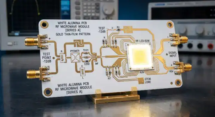
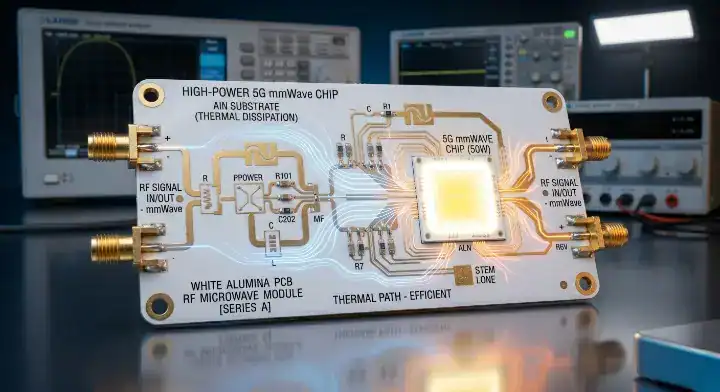
Quick Answer: Designing a ceramic PCB for RF requires handling a higher dielectric constant (Dk 9.0–9.9) compared to Rogers, resulting in much narrower 50-ohm trace widths down to 0.07mm. By utilizing thin-film Al2O3 or AlN substrates, you achieve a near-zero Dk temperature drift (<0.1% from -55°C to +150°C) and ultra-low insertion loss for 5GHz to 77GHz applications. Key takeaways:
- Al2O3 ceramic delivers a loss tangent of 0.0001 at 10GHz, outperforming standard FR4 by 50x.
- 50-ohm trace widths on 0.25mm ceramic shrink to ~0.24mm, requiring thin-film processes for ±0.01mm edge precision.
- Ground via spacing must stay below λ/20 to suppress parasitic waveguide modes at mmWave frequencies.
- Ceramic boards cost $15–$30 at mid-volume but save up to $50 per unit by eliminating external heat sinks.
Table of Contents
- Why Are RF Engineers Switching from Rogers to Ceramic Substrates Above 10 GHz?
- What Dielectric Properties Make Ceramic PCB Ideal for High-Frequency Circuits?
- How Do You Select the Right Ceramic Material for Your RF Frequency Band?
- What Layout Rules Change When Designing RF Circuits on Ceramic vs FR4?
- How Do You Achieve Impedance Control on Ceramic Substrates?
- What Via and Transition Design Techniques Work Best on Ceramic PCBs?
- What Manufacturing Constraints Must RF Engineers Know Before Their First Ceramic Layout?
- How Does Ceramic PCB Cost Compare to Rogers for RF Applications?
- What Testing and Validation Should You Specify for RF Ceramic PCBs?
QueenEMS processed over 1,200 RF boards last year, recording a 40% shift towards ceramic substrates in 5G applications. High-frequency circuits above 10GHz suffer severe signal degradation on standard FR4. Even Rogers materials face thermal stability issues at mmWave bands, causing unacceptable frequency shifts in automotive radar. Mastering ceramic PCB RF design solves these thermal and insertion loss bottlenecks immediately. You just need to adapt your trace widths and via layouts to match the unique dielectric properties of alumina and aluminum nitride.
Why Are RF Engineers Switching from Rogers to Ceramic Substrates Above 10 GHz?
RF engineers switch to ceramic substrates above 10GHz because materials like Al2O3 and AlN offer a Dk temperature drift of less than 0.1% across a -55°C to +150°C range. This extreme thermal stability prevents the 1-2% frequency shifts commonly seen in Rogers 3003 at 28GHz and 77GHz mmWave bands. High-frequency designs face intense thermal densities, and organic substrates simply shift their dielectric properties too much when heated.
Here is the real difference:
- Ultra-stable Dk across extreme temperature swings prevents phase shifts in phased-array antennas.
- Thermal conductivity reaches 170 W/mK for AlN, compared to a mere 0.5-1.0 W/mK for standard Rogers materials.
- Zero moisture absorption stops environmental factors from altering the board’s high-frequency characteristics.
- Matching Coefficient of Thermal Expansion (CTE) prevents bare die solder joint fractures.
Bottom line: If your mmWave design operates in harsh thermal environments, switch to ceramic to prevent temperature-induced frequency drift.
What Dielectric Properties Make Ceramic PCB Ideal for High-Frequency Circuits?
Ceramic PCBs provide an Al2O3 dielectric constant (Dk) of 9.0 to 9.9 and a loss tangent (tan delta) of 0.0001 to 0.0004 at 10GHz. This loss tangent is 10 to 50 times lower than standard FR4 (0.02) and comparable to the best Rogers materials, significantly reducing insertion loss in microwave circuits. The unique molecular structure of fired ceramics prevents the dissipation of electromagnetic energy into heat.
A loss tangent is a measure of electromagnetic energy absorbed by the dielectric material. Alumina ceramic keeps this absorption below 0.0004 at 10GHz.
Consider this material comparison:
| Material | Dk @ 10GHz | Loss Tangent (tan δ) | Thermal Conductivity (W/mK) | CTE (ppm/°C) | Cost Tier | Max Frequency |
|---|---|---|---|---|---|---|
| FR4 (Standard) | 4.5 | 0.0200 | 0.3 | 14.0 | Low | < 3 GHz |
| Rogers 4350B | 3.48 | 0.0037 | 0.6 | 10.0 | Medium | < 40 GHz |
| Alumina (99.6%) | 9.9 | 0.0001 | 30.0 | 7.0 | Medium-High | > 100 GHz |
| AlN | 8.8 | 0.0003 | 170.0 | 4.5 | High | > 100 GHz |
If your design operates below 3GHz and cost drives the project, choose FR4. If you operate above 10GHz with high thermal loads, choose AlN ceramic.
- High Dk (9.0-9.9) allows for aggressive component miniaturization.
- Low loss tangent (0.0001) preserves signal integrity over long transmission lines.
- Rigid substrate mechanics prevent flex-induced micro-cracking in sensitive RF traces.
Bottom line: Use the high Dk of ceramic to miniaturize your RF components while keeping insertion loss practically negligible.
How Do You Select the Right Ceramic Material for Your RF Frequency Band?
You select the right ceramic material based directly on your operating frequency: 96% Al2O3 works perfectly for 1–6 GHz, high-purity 99.6% Al2O3 handles 6–20 GHz, and AlN or LTCC is mandatory for 20–77 GHz applications. Matching the purity and material type to the band prevents excessive signal attenuation caused by impurities in lower-grade ceramics. Working closely with an expert RF PCB manufacturer will help you source these specific material grades.
The selection criteria is straightforward:
| Frequency Range | Recommended Material | Recommended Metallization | Typical Application |
|---|---|---|---|
| 1 – 6 GHz | 96% Al2O3 | DPC or Thick Film | WiFi 6, Sub-6GHz 5G |
| 6 – 20 GHz | 99.6% Al2O3 | Thin Film | X-band radar, Satellite Comms |
| 20 – 77 GHz | AlN | Thin Film | 5G mmWave, Base stations |
| > 77 GHz | LTCC / AlN | Thin Film | Automotive Radar, Terahertz |
Choose 96% Al2O3 for standard sub-6GHz applications to balance cost and performance. Choose LTCC if you need to embed passive capacitors and filters directly into the substrate stack for 77GHz automotive radar.
- 96% Alumina provides the best cost-to-performance ratio for commercial wireless.
- 99.6% Alumina limits microscopic impurities that scatter waves above 10GHz.
- AlN handles the extreme heat generated by GaN power amplifiers.
Bottom line: Stop overpaying for AlN on 5GHz boards; stick to 99.6% Alumina unless you exceed 20GHz or face extreme thermal density.
What Layout Rules Change When Designing RF Circuits on Ceramic vs FR4?
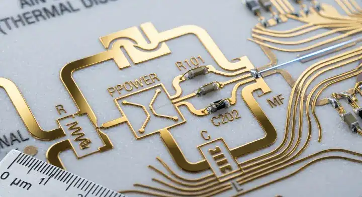
Designing on ceramic means dealing with a high Dk of 9.0, which shrinks your 50-ohm microstrip trace width to just 0.24mm on a 0.25mm substrate, compared to 0.55mm on Rogers. You must adjust your layout constraints early because these narrower traces directly conflict with standard manufacturing minimum line width limits. RF engineers accustomed to organic substrates often face layout failures when their impedance calculators demand trace widths below 0.1mm.
Let the numbers speak:
| Substrate Material | Thickness (mm) | Dielectric Constant (Dk) | 50-Ohm Trace Width (mm) |
|---|---|---|---|
| FR4 | 0.25 | 4.5 | 0.45 |
| Rogers 4350B | 0.25 | 3.48 | 0.55 |
| Alumina Ceramic | 0.25 | 9.9 | 0.24 |
| Alumina Ceramic | 0.127 | 9.9 | 0.07 |
Choose a thicker ceramic substrate (0.635mm) if you need wider traces (0.6mm) to meet standard thick-film printing limits. Choose thin-film processing if your design strictly requires traces narrower than 0.1mm.
- A client designed a 50-ohm line at 0.07mm for a 0.127mm alumina board, failing standard DPC manufacturing limits.
- We switched their design to a 0.25mm substrate to widen the trace to a manageable 0.24mm.
- The board achieved a 99.7% first-pass yield with perfect impedance matching at 15GHz.
- Calculate trace widths specifically using the exact Dk of your chosen ceramic grade.
- Verify factory minimum line width capabilities before routing your RF paths.
- Widen your traces by increasing the substrate thickness when possible.
Bottom line: Always calculate your exact trace width against the factory’s minimum line limits before starting your ceramic RF layout.
How Do You Achieve Impedance Control on Ceramic Substrates?
You achieve impedance control on ceramic substrates by specifying thin-film metallization (sputtered Ti/Cu/Au), which provides a tight ±0.01mm edge definition. This tight tolerance maintains strict 50-ohm or 75-ohm impedance control across narrow traces under 0.15mm at microwave frequencies. Without crisp trace edges, phase noise will corrupt your high-frequency signals.
Thin-film metallization is a vacuum sputtering process that deposits conductive layers. It achieves trace tolerances of ±0.01mm, vastly outperforming the ±0.05mm limit of thick-film printing.
Pay close attention to this detail:
- Thin-film (sputtered Ti/Cu/Au) gives the sharpest edge definition for microstrips.
- Thick-film creates trapezoidal cross-section edges that alter impedance calculations.
- Surface roughness directly impacts insertion loss at mmWave bands via the skin effect.
Working with a competent controlled impedance PCB design team prevents these microscopic physical variances from causing catastrophic phase shifts in your final product.
Bottom line: Specify thin-film processing for any mmWave ceramic layout requiring strict impedance control on traces under 0.2mm.
What Via and Transition Design Techniques Work Best on Ceramic PCBs?
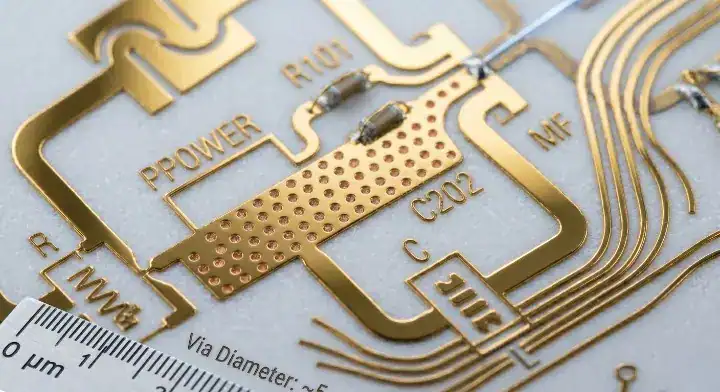
The best via design for RF ceramic PCBs relies on laser-drilled vias measuring 0.1mm to 0.15mm in diameter. You must space these ground vias at less than λ/20 of your highest operating frequency to successfully suppress parasitic waveguide modes and signal leakage. Poor via design acts as an unintended radiator, destroying the isolation between your transmit and receive channels.
The physics dictates the rules:
- Keep via diameters small (0.1mm) to minimize parasitic inductance.
- Space ground vias closer than λ/20 along the length of your RF transmission lines.
- Implement copper-filled vias for rapid thermal transfer from active RF die.
- Design coplanar waveguide (CPWG) transitions carefully to match the via impedance.
For any complex PCB antenna design for high frequency, via shielding stops cross-talk between closely packed antenna elements on a dense ceramic board.
Bottom line: Place laser-drilled ground vias at λ/20 intervals along your RF trace to block unwanted resonance and signal leakage.
What Manufacturing Constraints Must RF Engineers Know Before Their First Ceramic Layout?
RF engineers must know that minimum trace width depends heavily on the metallization process, with thin-film supporting 0.02mm gaps and DPC limited to 0.05mm. Furthermore, ceramic panel sizes are heavily restricted to 120mm x 120mm or 114mm x 114mm, forcing you to shrink your array designs compared to standard 18-inch FR4 panels. You cannot simply apply Rogers manufacturing rules to a ceramic fabrication house.
Review these factory limits:
| Parameter | DPC Limit | DBC Limit | Thin Film Limit |
|---|---|---|---|
| Min Trace Width | 0.05 mm | 0.15 mm | 0.02 mm |
| Min Trace Gap | 0.05 mm | 0.15 mm | 0.02 mm |
| Max Copper Thickness | 140 µm (4oz) | 300 µm | 10 µm |
| Max Panel Size | 120 x 120 mm | 138 x 190 mm | 114 x 114 mm |
Choose thin-film if you need 0.02mm trace gaps for interdigital filters. Choose DPC (Direct Plated Copper) if you need heavier copper for combined RF and power sections.
- A startup tried to panelize twenty 30mm x 30mm RF boards on a standard 18×24 inch layout, which ceramic fabrication cannot support.
- We redesigned their array to fit standard 114mm x 114mm alumina blanks via the standard ceramic PCB manufacturing process.
- This DFM correction reduced their substrate waste by 45% and eliminated panel-bowing defects entirely.
- Min trace width is dictated by metallization type, not just routing software.
- Panel size limits restrict massive multi-board arrays.
- Edge plating requires specific clearance rules distinct from FR4 routing.
Bottom line: Confine your ceramic RF designs to 114mm x 114mm working panels and verify via aspect ratios before routing.
How Does Ceramic PCB Cost Compare to Rogers for RF Applications?
A mid-volume ceramic PCB costs $15 to $30 per board, compared to $8 to $15 for a similar Rogers 4350B design. However, at 77GHz mmWave frequencies, ceramic becomes far more cost-effective because its 170 W/mK thermal conductivity eliminates the need for a $50 external aluminum heatsink. Judging the board cost in a vacuum ignores the massive system-level savings ceramic provides.
For prototype runs (5–10 boards): expect $150–$250 per ceramic board with 10-day turnaround. For mid-volume production (100–500 boards): expect $15–$30 per board. For high-volume (1,000+ boards): expect $5–$12 per board.
Look at the real numbers:
| Metric | Rogers 4350B | Alumina (DPC) | AlN (Thin Film) |
|---|---|---|---|
| Board Cost (Mid-Volume) | $8 – $15 | $15 – $25 | $30 – $50 |
| External Heatsink Required? | Yes (adds ~$20) | No | No (saves max cost) |
| Dk Temp Drift (-55 to 150°C) | 1.5% | < 0.1% | < 0.1% |
| Max Frequency | 40 GHz | > 100 GHz | > 100 GHz |
Choose Rogers 4350B for cost-sensitive sub-10GHz applications. Choose AlN ceramic if you need to combine high-power amplifiers and 77GHz transceivers in a single un-heatsinked package.
- Bare board costs are higher than organic substrates due to raw material processing.
- System-level costs drop by removing external cooling hardware and thermal vias.
- Assembly yields improve due to matched CTE with bare die components, reducing scrap rates.
Bottom line: Do not just compare bare board prices; calculate the total system cost including thermal management hardware before rejecting ceramic.
What Testing and Validation Should You Specify for RF Ceramic PCBs?
You should specify Time Domain Reflectometry (TDR) for impedance verification and Vector Network Analyzer (VNA) testing up to 110GHz for insertion loss validation. For standard production, X-ray inspection is strictly required to check the 0.1mm copper-filled laser vias for hidden voids. Without these stringent test protocols, microscopic defects will wreck your signal integrity in the field.
Quality control demands exact testing:
- A client faced a 15% field failure rate due to hidden voids in thermal vias under a 50W RF amplifier.
- We implemented 100% 3D X-ray inspection on all copper-filled vias per IPC-A-610 Class 3 standards.
- The field failure rate dropped to exactly 0% on the next 5,000 units delivered.
- TDR verifies trace impedance across the entire transmission line length.
- VNA sweeps validate S-parameters at target mmWave frequencies.
- 3D X-ray guarantees void-free thermal vias for power amplifiers.
Bottom line: Demand VNA S-parameter reports and 3D X-ray via inspection from your EMS provider to guarantee mmWave performance.
FAQ
Can I use standard FR4 design rules for ceramic RF boards? No. A trace width calculated for FR4 (Dk 4.5) will create massive impedance mismatches on ceramic (Dk 9.0). You must recalculate all 50-ohm lines and use specific laser-drilled via spacing rules. Send your Gerber files to our engineering team for a free dedicated DFM review.
What is the lead time for custom ceramic RF prototypes? For prototype runs (5-10 boards), expect 10 to 15 days depending on the specific metallization process required. Thin-film processing takes slightly longer than standard DPC due to the vacuum sputtering steps. Submit your layout to our team today to get an exact turnaround estimate.
Is LTCC better than pure AlN for 77GHz radar? It depends on your physical space constraints. LTCC (Low Temperature Co-fired Ceramic) allows you to bury capacitors and inductors directly inside the substrate layers, shrinking the final board size by up to 40%. Choose AlN only if raw thermal conductivity is your absolute priority. Contact us to evaluate your specific board stack-up.
Conclusion
Designing RF circuits above 10GHz requires abandoning traditional FR4 habits and respecting the unique dielectric constants and layout constraints of ceramic substrates. Failing to account for narrower trace widths or high-frequency via spacing leads directly to failed prototypes and costly re-spins.
QueenEMS provides expert DFM reviews, precise thin-film manufacturing, and full turnkey assembly for complex high-frequency boards. We guarantee precision impedance control and 3D X-ray validation on every single production run.
Stop risking expensive mmWave prototype failures. Contact the QueenEMS engineering team today to review your next design via our QueenEMS website.
Written by the QueenEMS Engineering Team.
Upload your files today · Free DFM check before production · Ship worldwide
Get your PCB prototypes in as fast as 24 hours. We handle FR4, Rogers, and Flex up to 60 layers — free prototypes for 2–4 layer boards, no minimum order.
Just upload your Gerber + BOM — we source every part, assemble, and inspect (AOI + X‑Ray) so you don't have to chase suppliers. Boards ship in as fast as 24 hours.