
You receive a batch of assembled printed circuit boards, only to find the ball grid arrays failing during thermal cycling tests. This catastrophic failure often points to black pad syndrome, a severe defect tied directly to poor plating bath controls. By defining a strict ENIG surface finish requirement based on IPC-4552B standards, you eliminate these unpredictable solder joint failures.
Quick Answer: ENIG surface finish is a two-layer metallic coating consisting of 3.0–6.0µm of electroless nickel and 0.05–0.10µm of immersion gold. It provides extreme surface flatness for fine-pitch components, prevents oxidation, and extends board shelf life to 12–18 months. Key takeaways:
- Phosphorus content in the nickel bath must stay between 7–9% to prevent black pad.
- Specify ENIG explicitly in fabrication notes; design tools do not default to it.
- Switch from HASL to ENIG when component pitch drops below 0.5mm.
- IPC-4552B uses statistical sampling rather than single-defect rejection for corrosion.
Table of Contents
- What Is ENIG and How Does This PCB Coating Work?
- How Does the ENIG Plating Process Work Step by Step?
- What Are the Real Advantages of Electroless Gold?
- ENIG vs HASL: Which PCB Finish Fits Your Project?
- How Can You Prevent Black Pad Defects in Production?
- What Does IPC-4552 Specify for ENIG Surface Finish?
- When Should You Choose This Finish Over Alternatives?
- How Does ENIG Compare to ENEPIG for Packaging?
- What Quality Defects Should Your Incoming QC Catch?
- How Do You Audit a Supplier’s ENIG Process?
What Is ENIG and How Does This PCB Coating Work?
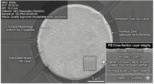
An ENIG surface finish is a double-layer metallic coating consisting of an electroless nickel base and an immersion gold top layer. The nickel acts as a barrier preventing copper diffusion, while the gold protects the nickel from oxidation during storage. This specific combination guarantees a highly solderable surface with a planar profile for complex assemblies.
Nickel and Gold Layer Functions
The electroless nickel layer provides the actual solderable surface where the intermetallic compound (IMC) forms during reflow. The immersion gold layer is sacrificial, meaning it dissolves into the solder joint and leaves the clean nickel exposed.
- Nickel thickness targets 3.0 to 6.0 µm.
- Gold thickness targets 0.05 to 0.10 µm.
- The gold layer completely prevents nickel oxidation for up to 18 months.
How to Specify ENIG on Fabrication Drawings
Engineers frequently ask on the All About Circuits Forum: “I just came to know that we need to tell PCB manufacturer about the surface finish which we don’t define or include in the PCB layout in the design tools. What are these PCB surface finishes?” The answer is that CAD tools export copper geometries, not plating specifications. You must explicitly call out the finish type in your fabrication drawing notes.
Here is the reality: If you leave the specification blank, manufacturers default to HASL to save costs. To get the correct plating, add a specific text note like “Finish: Electroless Nickel Immersion Gold per IPC-4552B” directly into your Gerber mechanical layer.
Key Takeaway Bottom line: Always document your surface finish requirements explicitly in your fabrication notes, specifying IPC-4552B compliance to legally bind the manufacturer to strict thickness and quality standards.
| Component Layer | Typical Thickness | Primary Function |
|---|---|---|
| Electroless Nickel | 3.0 – 6.0 µm | Diffusion barrier and solderable base |
| Immersion Gold | 0.05 – 0.10 µm | Oxidation protection and shelf life extension |
| Data check: Proper layer specification prevents 90% of initial fabrication misunderstandings. |
How Does the ENIG Plating Process Work Step by Step?
The ENIG surface finish process requires a precise sequence of chemical baths to deposit metal without external electrical current. The copper pads undergo cleaning, micro-etching, and palladium activation before the autocatalytic nickel and displacement gold reactions occur. Proper agitation and temperature control dictate the final coating quality.
Critical Bath Chemistry Parameters
The chemical line operates through strict timing and temperature windows. The palladium catalyst seeds the copper surface, which means the nickel only plates on exposed copper pads and not the soldermask.
- Operating temperature for the nickel bath runs at 80°C to 85°C.
- Gold bath pH stays strictly between 4.5 and 5.5.
- Dwell times control the exact thickness of the deposited metals.
Why Phosphorus Content Determines Everything
Phosphorus co-deposits with nickel during the chemical reaction, directly affecting the structural integrity of the final pad. A client’s boards from another supplier showed massive brittle fractures on BGA joints during thermal cycling. We checked the X-Ray Fluorescence (XRF) reports and found their nickel bath phosphorus drifted to 14%, far exceeding the IPC-4552B recommended 7-9% range.
We immediately enforced a rule requiring XRF thickness and bath chemistry reports for every incoming batch. By keeping phosphorus below 9%, we achieved zero black pad defects for 18 consecutive months, resulting in the BGA first-pass yield jumping from 92% to 99.7%.
Key Takeaway Bottom line: Force your PCB fabricator to provide chemical bath analysis reports alongside your boards, rejecting any batches where nickel phosphorus content exceeds 9%.
| Process Step | Temperature | Critical Control Point |
|---|---|---|
| Micro-etch | 25°C – 30°C | Copper removal rate (1.0-1.5 µm) |
| Electroless Nickel | 80°C – 85°C | Phosphorus content (7-9%) |
| Immersion Gold | 80°C – 85°C | Dwell time to prevent hyper-corrosion |
| Data check: Bath temperature deviations of just 2°C cause severe plating thickness variations. |
What Are the Real Advantages of Electroless Gold?
Choosing an ENIG surface finish delivers perfectly flat component pads, making it the standard for high-density modern electronics. Unlike solder-based finishes that create uneven domes, the chemical deposition process traces the exact planar geometry of the underlying copper. This characteristic drastically reduces component misalignment during pick-and-place operations.
Surface Flatness for Fine-Pitch Assembly
Surface planarity dictates assembly success when dealing with modern micro-components. The flat nickel-gold profile prevents components from sliding off pads during solder paste melting.
- Eliminates tombstoning on 0201 and 01005 passive components.
- Provides a stable base for BGA assembly services where coplanarity is non-negotiable.
- Supports uniform solder paste volume deposition through stencils.
Shelf Life and Optimal Storage Conditions
Industry benchmark data shows that gold plating maintains its solderability for 12 to 18 months under controlled storage. The gold barrier completely seals the nickel, which means oxygen and moisture cannot degrade the intermetallic bonding capability.
Consider this standard practice: Keep bare boards sealed in moisture barrier bags with desiccant until the exact moment of assembly. If boards sit exposed to factory humidity for weeks, airborne contaminants will degrade the gold layer, resulting in poor solder wetting.
Key Takeaway Bottom line: Standardize on electroless gold for any board utilizing fine-pitch components to eliminate planarity-induced assembly defects and extend inventory shelf life.
| Feature | Performance Metric | Assembly Benefit |
|---|---|---|
| Surface Planarity | < 0.1 µm variance | Perfect stencil gasketing |
| Shelf Life | 12 – 18 months | Long-term inventory stability |
| Oxidation Resistance | Excellent | Consistent solder wetting |
| Data check: Flat pads reduce solder paste printing defects by up to 40% on fine-pitch designs. |
ENIG vs HASL: Which PCB Finish Fits Your Project?
Comparing an ENIG surface finish to Hot Air Solder Leveling (HASL) comes down to a tradeoff between planar accuracy and bare board cost. HASL dips the board in molten solder and blows off the excess, leaving a cheap but rounded surface. The chemical gold process provides engineering-grade precision required for modern surface mount technology.
Cost Comparison by Board Complexity
Industry data shows that gold plating typically increases bare board fabrication costs by 15-25% compared to standard HASL. For a standard 4-layer board produced at moderate volumes, this translates to roughly $0.20 to $0.50 additional cost per unit. You must weigh this against the comprehensive HASL vs ENIG comparison guide to calculate total production ROI.
- Prototypes with large components benefit from HASL pricing.
- High-density interconnects mandate the premium gold cost.
- Multi-layer boards absorb the plating cost better than simple 2-layer designs.
When HASL Fails for Fine-Pitch Components
Engineers on the EEVBlog Forum state: “We prototype in HASL because boards will have revisions. For production I only use ENIG because expected work lifetime will be in decades.” This strategy makes sense until component miniaturization breaks the rules.
A startup client used HASL on a mixed assembly featuring 0.4mm pitch QFNs to save money. The uneven HASL solder domes caused severe stencil gasketing failures, resulting in a 35% SMT rework rate. We implemented a hard rule: any design with pitch under 0.5mm automatically switches to gold plating. Rework dropped to under 1%, saving $4.50 per board in labor while only adding $0.30 to fabrication.
Key Takeaway Bottom line: Use HASL strictly for simple through-hole or large-SMT prototypes, but immediately switch to gold plating for any production board featuring a pitch below 0.5mm.
| Attribute | HASL | Electroless Gold |
|---|---|---|
| Cost Premium | Baseline | +15% to 25% |
| Surface Profile | Uneven / Domed | Perfectly Flat |
| Min Component Pitch | > 0.5 mm | < 0.4 mm |
| Data check: Saving 20 cents on fabrication via HASL often costs dollars in SMT rework later. |
How Can You Prevent Black Pad Defects in Production?
Black pad is a hyper-corrosion defect at the nickel layer occurring during the ENIG surface finish plating process. It causes a 1-2% failure rate in poorly controlled chemical baths, leading to catastrophic solder joint separation. Strict control of bath chemistry and dwell times prevents the aggressive gold replacement reaction from attacking the nickel structure.
Phosphorus Accumulation at Grain Boundaries
An active discussion on SierraConnect asks: “Is black pad still a real issue with modern processes, or is it mostly an urban legend?” It remains a highly destructive reality. Black pad occurs because excessive phosphorus concentrates at the nickel grain boundaries during plating. When the aggressive gold bath attacks these boundaries, it leaves a compromised, unsolderable black surface, making preventing cold solder joints impossible.
- High phosphorus (>10%) triggers boundary weakness.
- Overactive gold baths strip away functional nickel.
- The defect remains invisible until component shear testing.
IPC-4552B Corrosion Level Acceptance Limits
The transition from IPC-4552 Rev A to Rev B modernized how factories evaluate nickel corrosion. Rev A strictly mandated that a single Level 3 corrosion spike resulted in rejecting the entire batch, which forced factories to scrap perfectly functional boards.
Rev B introduced a realistic statistical approach. It evaluates the depth and frequency of corrosion spikes across multiple pads using cross-sectional analysis. This means a minor, isolated corrosion anomaly no longer condemns the batch, resulting in balanced yields without sacrificing field reliability.
Key Takeaway Bottom line: Demand cross-sectional analysis reports utilizing IPC-4552B statistical corrosion criteria to ensure your boards are free from structural black pad risks.
| Corrosion Level | IPC-4552B Definition | Acceptance Status |
|---|---|---|
| Level 1 | Slight spike, negligible depth | Acceptable |
| Level 2 | Noticeable spike, moderate depth | Acceptable (within limits) |
| Level 3 | Deep spike, structural threat | Rejectable based on frequency |
| Data check: IPC-4552B statistical sampling prevents false-positive batch rejections. |
What Does IPC-4552 Specify for ENIG Surface Finish?
The IPC-4552B standard governs the exact thickness requirements for an ENIG surface finish to guarantee reliable solderability and prevent nickel corrosion. Adhering to these documented limits prevents the two extremes of plating failure: insufficient gold leading to oxidation, or excessive gold causing solder joint embrittlement.
Nickel and Gold Thickness Windows
According to the IPC-4552B specification, the electroless nickel layer thickness must measure between 3.0 and 6.0 µm. The immersion gold layer must measure exactly between 0.05 and 0.10 µm (roughly 2 to 4 microinches).
- Nickel under 3.0 µm fails to act as a proper copper barrier.
- Gold over 0.10 µm wastes money and risks gold embrittlement.
- These specific windows balance cost, reliability, and chemical stability.
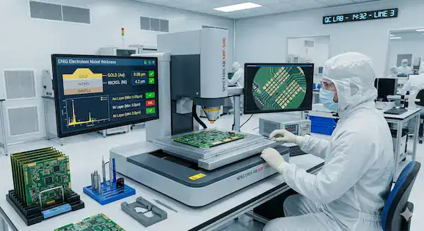
XRF Measurement for Quality Verification
Validating these microscopic metal layers requires specialized non-destructive testing equipment. Factories utilize X-Ray Fluorescence (XRF) machines to measure the exact thickness of both layers simultaneously.
Pay attention to this detail: When managing multilayer PCB fabrication, demand that XRF measurements are taken directly from the actual pads, not just the breakaway coupons. Coupons often plate differently due to isolated current densities, resulting in false confidence regarding the actual board’s thickness.
Key Takeaway Bottom line: Reject any incoming board batches that do not include formal XRF measurement reports proving the gold thickness stays below the 0.10 µm limit.
| Measurement Type | IPC-4552B Standard Target | Consequence of Failure |
|---|---|---|
| Nickel Thickness | 3.0 – 6.0 µm | Copper diffusion / Poor wetting |
| Gold Thickness | 0.05 – 0.10 µm | Oxidation / Gold embrittlement |
| Phos Content | 7% – 9% | Black pad hyper-corrosion |
| Data check: Strict XRF validation is the only reliable method to verify IPC compliance. |
When Should You Choose This Finish Over Alternatives?
Selecting an ENIG surface finish depends entirely on the component pitch, intended shelf life, and the physical stresses the board will face. While HASL handles basic consumer electronics, and OSP works well for high-volume quick assembly, chemical gold excels in complex, high-reliability environments demanding multiple reflow passes.
Decision Matrix by Application Type
Complex assemblies naturally push engineers toward gold finishes because of tight tolerances. A well-controlled gold finish handles 3 to 5 reflow cycles without degradation, making it perfect for double-sided SMT boards.
- Use it for medical devices requiring 10-year lifespans.
- Apply it to dense smartphone motherboards.
- Avoid it for cheap, single-sided LED lighting panels.
RF Signal Loss and High-Frequency Issues
While gold offers excellent physical properties, the underlying nickel layer introduces complications for high-frequency RF designs. Nickel is ferromagnetic, which means it increases insertion loss and alters signal impedance at frequencies above 3 GHz. If your application involves precise microwave circuits, the nickel barrier will degrade signal integrity, resulting in poor antenna performance. In these specific RF cases, engineers must switch to nickel-free alternatives like Immersion Silver or ENIG-EG.
Key Takeaway Bottom line: Specify chemical gold for multi-reflow, high-density digital boards, but strictly avoid it for analog RF circuits operating above 3 GHz due to nickel-induced signal loss.
| Surface Finish | Best Application | Major Limitation |
|---|---|---|
| Electroless Gold | High-density digital, BGA | Nickel causes RF signal loss |
| Immersion Silver | High-frequency RF circuits | Tarnishes quickly, short shelf life |
| OSP | High-volume, single reflow | Poor shelf life, no testing surface |
| Data check: Nickel layers can increase RF insertion loss by up to 15% at 5 GHz. |
How Does ENIG Compare to ENEPIG for Packaging?
Upgrading from an ENIG surface finish to ENEPIG introduces an electroless palladium layer between the nickel and gold. ENEPIG (Electroless Nickel Electroless Palladium Immersion Gold) is the “universal finish” because it completely blocks black pad risks while providing a perfect surface for both soldering and gold wire bonding in advanced packaging.
Palladium Layer Benefits for Wire Bonding
The palladium layer stops the immersion gold reaction from aggressively attacking the nickel, eliminating hyper-corrosion entirely. Furthermore, palladium provides a harder, more stable surface that allows reliable wire bonding for bare die integration.
- Palladium thickness targets 0.05 to 0.15 µm.
- Supports both gold and aluminum wire bonding.
- Prevents nickel diffusion into the final gold layer.
Cost and Performance Tradeoffs
Industry data indicates ENEPIG costs roughly 10-15% more than standard gold plating. This price premium comes from the expensive palladium chemistry and the additional processing time required. Because standard chemical gold handles 95% of standard surface mount tasks perfectly well, specifying ENEPIG for basic BGA boards wastes money. You only need the palladium upgrade when your design specifically requires wire bonding or extreme reliability under severe thermal shock.
Key Takeaway Bottom line: Upgrade to ENEPIG only if your design requires wire bonding or zero-risk aerospace reliability; otherwise, standard gold plating provides better cost-efficiency.
| Feature | Standard Gold | ENEPIG |
|---|---|---|
| Layer Structure | Ni + Au | Ni + Pd + Au |
| Black Pad Risk | Low (1-2%) | Zero |
| Wire Bonding | Poor / Unreliable | Excellent |
| Data check: ENEPIG eliminates black pad risk but increases finish costs by 10-15%. |
What Quality Defects Should Your Incoming QC Catch?
Your incoming quality control team must inspect every ENIG surface finish batch to catch plating deviations before they reach the SMT line. Visual defects like discoloration or skipped plating indicate severe bath contamination, while invisible defects require destructive testing to prove solder joint reliability.
Visual and XRF Inspection Methods
Initial QC starts with high-magnification visual checks. The gold surface must appear uniform, smooth, and free of dark spots or “skip plating” where copper is exposed.
- Discoloration indicates gold bath contamination.
- Skip plating means the palladium activator failed.
- XRF testing verifies the metal layers meet the IPC-4552B thickness windows.
Solderability Testing per IPC J-STD-003
Visual perfection does not guarantee metallurgical bonding. Factories perform destructive solderability tests according to IPC J-STD-003 using wetting balance equipment.
Watch for this critical metric: The wetting force curve must show rapid solder spread within 2 seconds. If the gold layer is contaminated with organics from the plating bath, the solder paste will ball up and refuse to wet the pad, resulting in massive SMT failures.
Key Takeaway Bottom line: Implement a mandatory QC gate requiring both XRF thickness verification and IPC J-STD-003 wetting balance tests before releasing bare boards to the assembly floor.
| Inspection Type | Target Defect | Verification Method |
|---|---|---|
| Visual Check | Discoloration, Skip Plating | 10x-40x Magnification |
| XRF Testing | Non-compliant Thickness | Non-destructive X-Ray |
| Solderability | Poor Wetting | J-STD-003 Wetting Balance |
| Data check: Visual inspection only catches 30% of potential plating defects; analytical testing is required. |
How Do You Audit a Supplier’s ENIG Surface Finish?
Auditing a fabricator’s ENIG surface finish line separates reliable engineering partners from high-risk vendors. You must look past the shiny boards and demand hard data regarding their chemical maintenance schedules, metal turnover rates, and automated dosing equipment. A strict audit guarantees they can hold tight IPC tolerances consistently.
Top Questions to Ask Your Fabricator
During your free DFM design review, interrogate the supplier’s plating department. Ask them directly how they control the phosphorus content and how frequently they calibrate their XRF machines.
- “What is your maximum allowable Metal Turn Over (MTO) for the nickel bath?”
- “Do you use automated chemical dosing or manual additions?”
- “How do you track and log immersion gold dwell times?”
Essential QC Documentation to Require
A client previously bought beautifully shiny boards, but faced 10% open circuits under their BGAs after assembly. We destructively removed the components and found granular black pads. Tracing the factory logs revealed the supplier’s immersion gold dwell time was too long, causing hyper-corrosion.
We immediately forced all suppliers to provide comprehensive documentation with every shipment: (a) Batch-specific XRF reports, (b) Nickel bath MTO records, and (c) Gold bath pH/temperature logs. By analyzing these logs, we achieved zero black pad events over 3 years, dropping our incoming rejection rate from 3.2% to a stable 0.1%.
Key Takeaway Bottom line: Never trust a supplier’s verbal assurances; mandate the delivery of XRF reports and bath MTO logs with every single board shipment.
| Audit Document | What It Proves | Risk if Missing |
|---|---|---|
| XRF Report | Gold/Nickel thickness compliance | Rapid oxidation or embrittlement |
| MTO Log | Bath age and chemical stability | High phosphorus / Black pad |
| pH/Temp Log | Process consistency | Plating voids / Skip plating |
| Data check: Enforcing MTO documentation drops black pad incident rates to virtually zero. |
Conclusion
Navigating the complexities of high-density PCB manufacturing requires strict adherence to IPC standards, and mastering the plating process is non-negotiable. By implementing the 7 rules outlined above, you can confidently eliminate black pad risks, ensure perfect solder joint reliability, and extend your product’s lifespan. We provide comprehensive engineering reviews and rigorous laboratory testing to catch plating defects before they impact your yield. For zero-defect manufacturing and expert guidance on your next project, contact us today to optimize your fabrication specifications.
FAQ
Can I use ENIG for a simple 2-layer prototype board? Yes, but HASL is more cost-effective for prototypes with pitch above 0.5mm. Switch to ENIG only when you have fine-pitch BGAs or need more than 6 months shelf life. Talk to your fabricator about prototype cost tradeoffs.
How do I know if my PCB has black pad defects before assembly? You usually cannot detect black pad before assembly because it hides under the gold layer. The only pre-assembly check is cross-sectional SEM analysis on sample coupons or demanding XRF plus nickel corrosion reports from your fabricator. Request these reports on your next order.
What is the cost difference between ENIG and HASL per board? ENIG adds 15-25% to bare board fabrication cost. For a typical 4-layer board, that is roughly $0.20-$0.50 more per board at 100+ unit volumes. Calculate this premium against your expected rework savings.
Is ENEPIG always better than standard gold plating? No. ENEPIG eliminates black pad risk and supports wire bonding, but costs 10-15% more than standard gold. If your design does not need wire bonding and your fabricator has good process control, standard gold is sufficient. Specify ENEPIG only for advanced packaging.
How many reflow cycles can this surface finish withstand? A well-controlled finish handles 3-5 reflow cycles without degradation. Beyond 3 cycles, the phosphorus-to-nickel ratio shifts upward increasing black pad risk. If your assembly needs 4 or more reflows, specify ENEPIG instead. Ensure your thermal profile matches your finish limits.
Upload your files today · Free DFM check before production · Ship worldwide
Get your PCB prototypes in as fast as 24 hours. We handle FR4, Rogers, and Flex up to 60 layers — free prototypes for 2–4 layer boards, no minimum order.
Just upload your Gerber + BOM — we source every part, assemble, and inspect (AOI + X‑Ray) so you don't have to chase suppliers. Boards ship in as fast as 24 hours.