Quick Answer: Read the wire bond solder mask window by its named edges: E runs from the root-side mask opening edge to the lead tip, while D runs from that tip to the opposite mask edge in Samtec’s illustrated convention. Moving the window along the lead trades one dimension against the other. Before release, agree on the edge mapping, value basis, opening form and permitted CAM changes.
A bond lead can continue underneath mask at its root while its tip ends inside an opening. That geometry needs a more specific description than “expand the pad.” The following reading uses one organic-substrate drawing from a 2017 vendor guideline. It supplies a drawing convention, not a current process capability or a requirement for a selected substrate.
What does the solder mask window around a wire-bond lead control?
The window defines where mask stops around the lead and which copper remains exposed in the illustrated opening. In the organic-substrate example, that exposure has a mask boundary at the root side and a copper boundary at the tip. The drawing therefore needs named edge pairs, rather than an unspecified clearance around a pad.
Keep that window definition with the selected lead drawing. A change to a mask edge can change the exposed lead length even when the copper outline stays fixed. The source does not turn that geometric observation into a bond-performance result.
Which edges do the D and E dimensions actually measure?
Both arrows run along the lead. E starts at the inner edge of the left mask column and ends at the lead's free tip. D starts at that tip and ends at the inner edge of the opposite mask column. An unlabelled lighter area sits in line with the lead inside the left mask column; no dimension describes it.
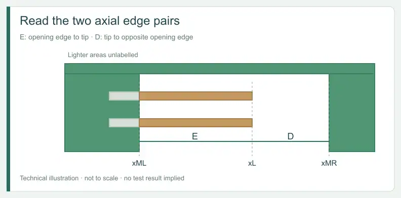
Check the top-down view in Samtec's 2017 fine-pitch wire-bond guideline. Its E label says “overlap,” yet the arrow runs from the opening edge to the lead tip; it does not measure any length under mask. Follow the drawn endpoints rather than the label word.
D/E edge-pair reading key
| Field | Source wording or gap | Edges and axis | Buyer disposition |
|---|---|---|---|
| D | “Space Solder Mask to Wire Bond Lead Edge”; organic minimum 0.004 in (100 µm) | Tip to opposite mask opening edge; along lead | Map project edges and value basis |
| E | “Overlap of Wire Bond Lead Edge to Solder Mask”; organic minimum 0.008 in (200 µm) | Root-side mask opening edge to tip; along lead | Map project edges and value basis |
| Lateral mask clearance | No transverse mask-clearance value given | Across lead, outside D/E axis | Define on project drawing |
| Lead beyond opening edge | Unlabelled lighter area; no length given | Root side, beyond the opening edge | Define if controlled |
| Between-lead mask | No web drawn between the two leads | Shared window as illustrated | Confirm project opening form |
Why is a bond-lead window not a uniform pad expansion?
A uniform expansion describes an opening around a pad perimeter. This example instead measures along a lead whose exposed length begins at a mask edge and whose tip ends inside a shared window. E has a mask edge at one end and a copper edge at the other; D measures the remaining gap on that same axis.
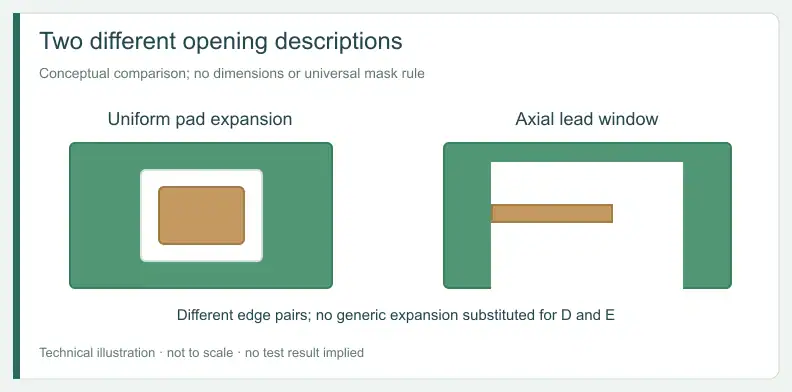
The guide to setting uniform mask expansion and dams for soldered pads covers the broader pad model. Do not use one expansion entry to stand in for this bond-lead window's two axial edge pairs. The source shows no inter-lead web; it does not explain why that opening form was chosen.
What does the drawing leave undimensioned?
The drawing gives no mask clearance across the lead, no length beyond the root-side opening edge, and no dimension to the mask band above the leads; it does not show where the opening ends below them. The blue marker and lighter shade have no legend, so neither establishes a wire landing position, bond footprint or process feature.
Treat each omission as a drawing question. Likewise, no conclusion follows from the ceramic column's missing D/E values. It gives no value and no explanation. Record the project requirement or an unresolved item rather than interpreting a blank as permission to omit a control.
What happens to D and E if the mask window shifts?
With the copper fixed, moving both mask edges in the root-to-tip direction shortens E and increases D by the same amount. Their sum, the window width along that axis, stays unchanged. This is a one-axis geometric reading aid. It does not model registration capability, two-dimensional tolerances, rotation, scaling or lead-tip etching.
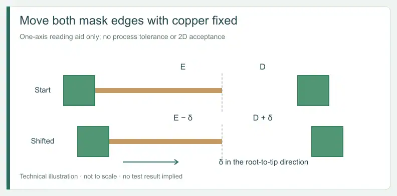
Label the root-side opening edge xML, the copper tip xL and the opposite opening edge xMR. Then E = xL − xML and D = xMR − xL. For a mask translation δ in the root-to-tip direction, E′ = E − δ and D′ = D + δ; W = D + E stays fixed.
If both dimensions were designed exactly at minimums that apply to the finished board, any shift in either direction would take one of them below its minimum. The source does not say whether its minimums describe design data or finished boards. Resolve that basis before using the aid in a project decision.
Which records tie the solder mask window to the selected bond lead?
Use the controlled drawing to connect each D/E-style callout with the selected lead, then obtain the supplier's CAM interpretation of that window. Record whether values control design data or the finished board. Any as-built check is a project requirement to specify, not a test method established by this source drawing or its example dimensions.
Window release record
These are buyer suggestions for closing a drawing definition, not reported test results.
| Check | Evidence that answers it | Provider | Evidence type | If missing |
|---|---|---|---|---|
| Edge mapping | Marked lead and mask endpoints | Package owner | Buyer suggestion | Confirm |
| Value basis | Guideline or project requirement identified | Package owner | Buyer suggestion | Hold |
| Design or finished board? | Meaning stated beside callout | Package owner / supplier | Buyer suggestion | Confirm |
| Allowed movement | Direction and applicable constraint, or unknown | Package owner / supplier | Buyer suggestion | Record |
| Opening form | Shared or per-lead window identified | Package owner | Buyer suggestion | Confirm |
| CAM permissions | Allowed changes and approval boundary | Package owner / supplier | Buyer suggestion | Hold |
| Finish decision | Responsible bonding or finish owner named | Bonding owner | Buyer suggestion | Confirm |
| Revision link | Matching mask, copper and drawing revisions | Package owner / supplier | Buyer suggestion | Hold |
What should the substrate RFQ package include for the window?
Include the mask and copper data, stackup and controlled drawing with the bond-lead window's edge pairs marked. State value origins, whether the opening is shared, and which CAM changes require approval. Keep the finish and bond-method decision with its named owner so the window definition is not mistaken for approval of the complete assembly.
The separate guide to grouping ENEPIG finish evidence for bond and solder pads addresses that finish decision. This window reading supplies no finish choice or bond-method recommendation.
Frequently Asked Questions
Is D the same as solder mask expansion?
No. In this drawing, D is one axial gap from the lead tip to the opposite mask opening edge. It is not an all-around expansion value.
Do the organic values establish BT substrate requirements?
No. The source does not establish that applicability. The selected construction and its requirements need project-specific confirmation.
Can one mask window span a bond row?
The source draws no web between its two leads. Whether a project uses a shared window is a drawing decision; the illustration supplies no universal rule.
Does the marker show where the wire lands?
The marker has no legend in this drawing. Do not use it to define a wire landing location or bond footprint.
Send your released files for a quote and free DFM review.
Send Gerber and the bond-lead and solder-mask-window drawing for review. Mark the finished exposed areas and the dimensional acceptance requirements.
If wire bonding or component assembly is requested, identify the parts and bond-pad requirements. Ask us to confirm the supported scope separately.