
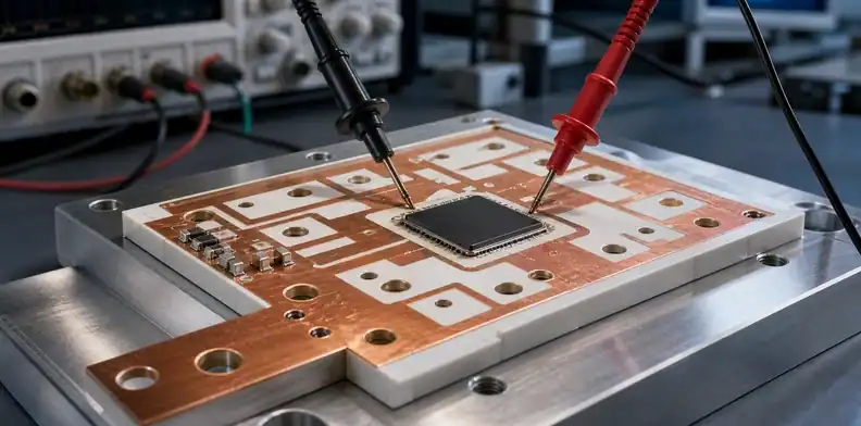
Quick Answer: Ceramic PCB dielectric strength is not a stand-alone purchasing number for a power module. The insulation decision must connect substrate material, ceramic thickness, metallization route, copper geometry, creepage and clearance, assembly interfaces, and the defined withstand or insulation-resistance test. A high material value cannot compensate for an unapproved finished construction or an undefined measurement boundary.
- Mistake 1: treating a material breakdown value as a module voltage rating.
- Mistake 2: choosing a ceramic grade before identifying the isolation path.
- Mistake 3: changing thickness without reviewing copper-edge and surface geometry.
- Mistake 4: swapping metallization routes without reviewing the changed construction.
Mistake 5 is accepting a test report without checking what it measured. The five technical sections below explain these errors; the RFQ and release sections show how to document the resulting decisions. A module contains copper geometry, ceramic thickness, interfaces, mounting and a voltage waveform, so the insulation review must address the complete construction.
The ceramic substrate selection page maps material and process choices. Here, the focus is how to specify and compare insulation evidence for a defined power-module construction.
Table of Contents
- What dielectric strength means in a ceramic PCB construction
- Why material selection is only the first insulation decision
- How thickness, copper edges, and geometry change the result
- What DBC, AMB, and DPC change in the review
- How creepage, clearance, and insulation tests differ
- What belongs in a power-module RFQ
- How to close the qualification and release record
What dielectric strength means in a ceramic PCB construction
Dielectric strength is the breakdown electric field reported for a specimen under stated test conditions, commonly expressed in kV/mm. It is not the same as the voltage applied across a complete module. Ceramic thickness, electrodes, surrounding medium and the voltage procedure must accompany the material result; the assembly adds copper edges, surface paths and interfaces.
The buyer should therefore avoid a vague request such as “high insulation.” State the voltage type, peak and continuous condition where relevant, expected environment, test method, test duration, measurement location, and acceptance action. A supplier can then determine whether the proposed construction needs a material change, geometry change, test coupon, or a formal qualification review.
Dielectric strength also does not replace system-level insulation design. A substrate may have favorable bulk properties while the module fails at an edge, a narrow surface gap, a contaminated interface, or a mounting feature. The construction must be reviewed as a whole.
Why material selection is only the first insulation decision
Alumina, aluminum nitride, and silicon nitride each bring different thermal, mechanical, and sourcing trade-offs. Their choice may be driven by heat flux, thermal cycling, mechanical strength, cost, or electrical isolation. The material matters, but it does not independently define the module’s insulation performance.
Start by identifying the actual power-module function. Is the ceramic used as an isolated baseplate substrate, a driver-board substrate, a high-voltage spacing element, or a thermally conductive submount? The answer changes the voltage path, test point, copper layout, and acceptance evidence. A general thermal board may need a different insulation definition from a traction inverter substrate.
| Decision input | Why it matters | What to specify |
|---|---|---|
| Substrate material and grade | Sets thermal and mechanical starting point | Named material family and approved option |
| Ceramic thickness | Changes bulk dielectric path and heat path | Finished thickness and tolerance |
| Voltage condition | Defines the insulation duty | AC/DC/pulse boundary and peak condition |
| Metallization route | Changes copper bond and geometry | DBC, AMB, DPC, or other approved route |
| Test method | Makes acceptance measurable | Withstand, insulation resistance, or project method |
For the material trade-off before the insulation review, see ceramic PCB thermal conductivity. Thermal performance is central to power modules, but it should not be allowed to erase the separate insulation decision.
How thickness, copper edges, and geometry change the result
Ceramic thickness changes the bulk path through the substrate, but the finished insulation condition also depends on copper geometry. Sharp copper features, small gaps, edge proximity, cavities, and localized contamination can create a field concentration or surface path that is not described by the bulk material number. The drawing should identify critical voltage separation and any feature that controls the test boundary.
Thickness creates a trade-off. A thicker ceramic may change the insulation path and mechanical behavior, while a thinner ceramic can improve some thermal paths but reduce the available dielectric distance. The right choice depends on the module layout, copper route, heat sink, and qualification target. Do not alter thickness to solve only one side of that trade-off without reviewing the other.
Copper also contributes to field shape and heat spreading. Heavy copper, etched geometry, and metallization edges should be reviewed alongside clearance and creepage requirements. A mechanical drawing or layer artwork that clearly marks high-voltage regions gives the supplier a chance to flag a construction risk before fabrication.
For a broader high-voltage drawing review, use high-voltage PCB requirements. The ceramic construction needs an additional material and metallization layer of evidence.
What DBC, AMB, and DPC change in the review
DBC, AMB, and DPC describe different ways of forming conductive features on ceramic substrates. They affect copper thickness options, bond interfaces, routing capability, mechanical behavior, and the kinds of process evidence a buyer should request. They should not be treated as interchangeable abbreviations in a quotation.
For a power module, DBC or AMB may be considered where durable copper attachment and thermal-cycling behavior are central. DPC can serve finer-feature constructions where metallization detail matters. The right construction depends on the module’s voltage, current, heat load, geometry, and manufacturing route. A request for “ceramic PCB” without the intended metallization path leaves too much open for a comparable quote.
The DPC versus DBC ceramic PCB comparison helps frame that process choice. For high-load modules, compare it with ceramic PCB for IGBT and SiC power modules so thermal cycling and isolation are considered together.
How creepage, clearance, and insulation tests differ
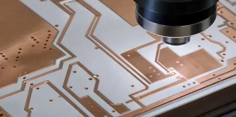
Clearance is the shortest air path between conductive parts; creepage is the shortest path along an insulating surface. Dielectric breakdown testing probes failure under a defined electrical stress, while insulation resistance measures resistance under a specified applied voltage and conditioning. These terms should appear as separate requirements in the drawing and test plan.
Which Test Does the Report Actually Describe?
| Evidence | What the result establishes | Conditions needed for comparison |
|---|---|---|
| Withstand or proof test | Whether the stated construction met the chosen acceptance criteria at the applied voltage | AC/DC or waveform, applied voltage, duration, leakage/trip criteria and test boundary |
| Breakdown voltage / dielectric strength | Failure voltage for the specimen; field strength uses its measured thickness | Thickness, electrode geometry, conditioning, surrounding medium, voltage rise procedure and failure criterion |
| Partial-discharge measurement | Localized discharge activity under a defined voltage sequence; not proof of complete breakdown | Measurement circuit, calibration, background noise, voltage sequence and agreed apparent-charge acceptance criterion |
For ASTM D149-25, the public scope and significance section explain why specimen conditioning, electrodes and voltage application must be controlled and why the result cannot usually be transferred directly to an application. It addresses commercial-power-frequency testing; do not label a DC result D149 without an applicable separate method.
IEC 60270:2025 addresses charge-based partial-discharge measurement. A withstand pass does not by itself report partial-discharge activity. Request a separate PD result when required by the module specification, including the calibrated measurement basis; this article does not prescribe a universal pC limit.
Write the requirement in the same language as the approval. If the product needs a withstand test, define the voltage, duration, location, and pass/fail action. If it needs insulation resistance, define the test condition and acceptance threshold. If layout distances are controlled by a safety standard or product requirement, preserve those dimensions in the drawing rather than assuming a material selection covers them.
The supplier should not choose the system safety boundary alone. Engineering or the compliance owner must supply the applicable requirement, while the fabricator confirms whether the physical ceramic construction can support it. That division prevents a quotation response from being mistaken for a compliance certification.
Environmental conditions should be named as well. Humidity, contamination, altitude, potting, enclosure geometry, and repeated high-temperature operation can change the relevance of a surface path or interface. A ceramic substrate is not an automatic waiver for those system conditions. The module owner should provide the environment; the supplier should identify which construction details need control in response.
Review Fast Switching and the Tested Interface
A sinusoidal PD result needs a separate applicability review before it supports a substrate exposed to fast, repetitive switching. Compare voltage amplitude and its definition, polarity, rise and fall times, repetition rate, pulse width and overshoot at the specimen. Equal nominal voltage does not make those electrical stresses equivalent.
In their 2024 ceramic-substrate experiments, Semenov and colleagues compared sinusoidal and switched excitation with substrates surrounded by silicone gel, silicone liquid or mineral oil. They reported lower PD inception voltage under switched excitation for their test objects, with differences between surrounding media. Those results support checking waveform and medium; they do not supply a conversion factor or acceptance voltage for another module.
Keep the stressed interface visible in the comparison. Record copper-edge geometry, lateral gaps, ceramic thickness, encapsulant and its preparation, environmental conditioning, and which conductors form the tested voltage path. Sherriff and colleagues’ DBC experiments used fast unipolar pulses and controlled humidity. They identified a humidity-sensitive weaker discharge group attributed to the gel or triple junction in the lateral copper trenches. Their observations describe those prepared, gel-encapsulated DBC specimens.
When artwork or encapsulation changes, mark the affected voltage paths and ask the qualification owner whether the earlier specimen represents them. The test laboratory should explain how its detection method separates discharge activity from switching interference at the specified stimulus. Preserve its measurement units and detection basis; a sensor-voltage result cannot be treated as an apparent-charge value without a demonstrated measurement relationship.
Illustrative document review: A prototype report covers a gel-encapsulated substrate under sinusoidal voltage. The production proposal changes a copper trench and uses fast switching. Attach both copper drawings, the encapsulation description and the intended specimen waveform to the review. Ask which changed region the old electrodes stressed and what evidence addresses the new condition. Retain the earlier result for its documented construction; approve its reuse only for paths and conditions the qualification owner can justify.
What belongs in a power-module RFQ
A usable RFQ identifies the ceramic material candidate, metallization route, finished thickness, copper thickness and pattern, outline, critical voltage regions, expected power or heat path, assembly method, and required evidence. Add the intended test condition and whether a prototype, qualification lot, or production lot must provide it.
For a SiC or IGBT module, include the thermal cycle or operating condition that may load the copper-to-ceramic interface. For an EV or high-voltage application, include the voltage duty and any project-specific clearance or creepage dimensions. For an optical or RF construction, state the local geometry that changes the field path. The supplier can then return questions that belong in the approved drawing rather than making an unrecorded assumption.
Use ceramic PCB CTE and thermal stress control when the insulation construction also faces thermal mismatch. Insulation evidence and mechanical reliability evidence should meet at one named construction revision.
How to close the qualification and release record
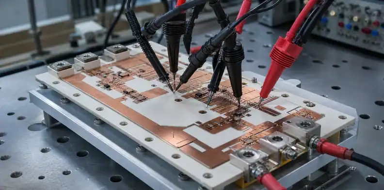
Put each voltage boundary on the drawing and connect it to a construction revision, test method and result. If the copper pattern or ceramic thickness changes, the reviewer can then identify which earlier results remain applicable and which require further evidence.
Close the release with a construction record that names the substrate, thickness, metallization route, copper geometry, test requirement, test result or qualification plan, and any supplier-approved process notes. Link the record to the drawing and purchase-order revision. This makes it possible to identify when a later quote changes the very features that created the original insulation approval.
Define the specimen drawing and electrode boundary before the lot is built. A generic material certificate does not demonstrate that a particular copper pattern, ceramic thickness and assembled interface have been evaluated. Keep the report beside the drawing it represents.
Review Two Reports That Seem to Disagree
Consider this illustrative document review. One supplier offers a breakdown result for an unmetalized material specimen; another offers a withstand pass for a patterned copper-clad substrate. Neither report is necessarily wrong, but their numbers answer different questions. The first can support material characterization. The second describes survival of a specified voltage exposure on its tested construction. Do not rank the suppliers by whichever number is larger.
First, compare the specimen drawings. Check thickness, electrode contact area, edge distance, metallization and any coating or encapsulation. Second, compare the electrical procedure: waveform, voltage rise, hold duration and trip criterion. Third, check conditioning and surrounding medium. A missing field is a request for clarification; it is not a measurement to fill in from a typical datasheet.
Next, map each report to the intended module boundary. A copper-to-copper surface path is different from isolation through the ceramic to a baseplate. If the report does not include the intended mounting or interface, ask which additional evidence addresses it. Finally, record whether the report is accepted for that specific requirement, accepted as background only, or requires a representative test. This decision keeps a useful material report in the file without overstating what it approves.
Keep the insulation record separate from unsupported compliance language. A fabricator can confirm the board construction, a stated test, and the documented result. Product-level certification, application safety analysis, and final installation approval remain with the product owner and the applicable compliance process. This separation makes the RFQ more credible and prevents a board-level report from being used outside its stated scope.
For a repeat module, review changes in ceramic supplier, material grade, thickness, copper pattern, metallization route, or test condition as potential construction changes. A familiar DBC or AMB label does not prove that the new build matches the original insulation evidence.
Consider a module that changes from a prototype copper pattern to a production layout with tighter high-voltage features. The ceramic material may remain the same, yet the field distribution, surface paths, and test locations can all change. Reusing a prototype dielectric-strength statement without reviewing the new artwork would leave the most important construction change outside the approval record.
The same caution applies to supplier alternatives. A different ceramic grade or metallization path may improve cost or lead time, but it can change thickness availability, copper edge definition, bond interface, or the appropriate test specimen. Ask the supplier to identify those differences in the quote response. The product owner can then decide whether the change fits the existing qualification or requires a new sample.
For a project with several voltage domains, identify each test boundary separately. One isolation path may run through the ceramic substrate, another across a surface gap, and another through an assembled interface. Combining them into one unsupported “high voltage” claim makes acceptance ambiguous. A clear drawing and test plan let engineering assign each path to a specific construction feature and result.
QueenEMS can review a ceramic power-module RFQ when you provide the voltage condition, substrate candidates, thickness, metallization route, copper artwork, thermal path, assembly method, and requested test evidence. The review can identify unclosed insulation assumptions before the quotation becomes a production release. Send the package through the QueenEMS contact page.
| Insulation term | Physical path to check | Release evidence |
|---|---|---|
| Bulk dielectric strength | Through the ceramic thickness | Material data for the named ceramic and thickness |
| Creepage | Along the finished surface | Dimensioned drawing and contamination/coating assumptions |
| Clearance | Through air between conductors | Assembly geometry and applicable spacing rule |
FAQ
Does a higher dielectric-strength material automatically make a safer module?
No. Bulk material performance is only one part of the finished insulation path. Copper geometry, ceramic thickness, surface distances, interfaces, contamination control, and the specified test condition also matter.
Should I specify DBC or AMB before asking for a quote?
Specify the intended route when it is a design requirement. If it remains open, ask the supplier to state the proposed route and explain how it affects copper, thickness, thermal cycling, and insulation evidence.
Can a thermal test replace a withstand test?
No. Thermal testing and electrical insulation testing answer different questions. A power-module qualification may need both, with each tied to the same construction revision.
What is the most useful first input for a ceramic insulation review?
The voltage and construction drawing. Include the ceramic thickness, copper pattern, material candidate, metallization route, and the actual test or acceptance requirement.
Sources
Written by the QueenEMS Engineering Team
Upload your files today · Free DFM check before production · Ship worldwide
Get your PCB prototypes in as fast as 24 hours. We handle FR4, Rogers, and hybrid boards up to 40 layers in volume production, with advanced builds subject to engineering review — free prototypes for 2–4 layer FR-4 boards, no minimum order.
Just upload your Gerber + BOM — we source every part, assemble, and inspect (AOI + X‑Ray) so you don't have to chase suppliers. Boards ship in as fast as 24 hours.