
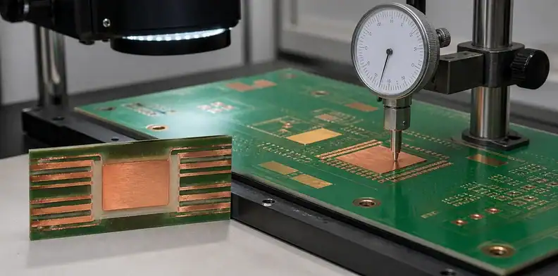
Quick Answer: An embedded copper coin PCB should be released only after the coin geometry, cavity relationship, bonding method, surface coplanarity, copper connection, thermal path and inspection evidence are defined. The supplier needs a dimensioned insert drawing and a controlled section through the coin interface, not just a note that says “add copper coin.” Acceptance must distinguish thermal performance from mechanical fit because a coin can be thermally promising yet unsuitable for component mounting or repeat production.
Embedded copper inserts create a short, highly conductive path through selected regions of a multilayer board. They also introduce an interface that ordinary PCB stack-ups do not have: a separately made metal part must fit, bond, laminate and finish as part of the panel without leaving unacceptable height, voids, distortion or registration error.
That makes the quotation a construction review rather than a simple material surcharge. Buyers should compare how each supplier proposes to build and verify the insert, then freeze the approved architecture before tooling.
Table of Contents
- When Should You Choose a Copper Coin Instead of Thermal Vias?
- Copper Coin PCB vs IMS PCB: What Should Buyers Compare?
- Define the insert and cavity as one interface
- Build a realistic dimensional tolerance chain
- Control bonding, resin flow and lamination
- Specify flatness and planarization at the surface
- Prove the electrical and thermal path
- Choose evidence and lot disposition
- What Files Do You Need for a Copper Coin PCB Quote?
When Should You Choose a Copper Coin Instead of Thermal Vias?
Choose a copper coin when a localized heat source needs a through-board metal path that a practical thermal via layout cannot provide within the temperature and space limits. Retain thermal vias when the assembled design already meets its thermal target. Device wattage alone does not establish which construction is needed.
Thermal vias conduct heat between copper layers, while copper planes spread it laterally. Via diameter, wall plating, quantity, board thickness and connection to useful copper area affect that path. Texas Instruments discusses these layout factors for power-device cooling. Adding vias outside the effective heat-transfer region should not be assumed to solve a constrained device footprint.
A coin can place a solid copper region beneath the hot component while retaining multilayer routing elsewhere. However, its benefit still depends on the device attachment, any required insulating layer, and contact with the heat sink. NXP AN1908 describes local coins as part of the thermal and electrical carrier path for specific RF power packages; it does not establish a universal coin specification for every PCB.
- Define device power loss, contact area, allowable temperature and the actual cooling conditions.
- Evaluate the via option using the intended plating, copper layers and available footprint, rather than an idealized array.
- Evaluate the coin option with its real attachment and heat-sink interfaces, including insulation where required.
- Validate the selected construction in the assembled product under the same operating conditions.
Illustrative design review: A multilayer controller has one hot power device and a heat sink below it. If the device-to-board region dominates the modeled temperature rise and the available via area is constrained, investigate a coin. If the main loss occurs at a poorly seated heat-sink interface, correct that interface first and re-evaluate both board options. This is an engineering example, not a reported QueenEMS customer result.
Copper Coin PCB vs IMS PCB: What Should Buyers Compare?
A copper coin addresses a selected board region; a conventional IMS PCB uses a circuit layer, an insulating dielectric and a metal base across the board. Compare the required circuit construction and complete cooling path before choosing between them. Neither copper conductivity nor an aluminum-base label predicts the finished assembly temperature.
| Buyer question | Embedded copper coin PCB | Conventional IMS PCB |
|---|---|---|
| Where must heat leave? | Define each local insert and its exit surface. | Define heat transfer through the dielectric to the metal base. |
| What routing must remain? | Check routing and isolation around the coin in the multilayer stack. | Confirm the required layer count and interconnections with the proposed IMS construction. |
| What provides electrical isolation? | Identify connected coin faces and any controlled dielectric separation. | Specify dielectric grade, thickness and the required isolation test. |
| Which surfaces meet the heat sink? | Control insert height, flatness and contact area. | Control base flatness, mounting and thermal-interface coverage. |
| What manufacturing evidence matters? | Request coin fit, bond-interface and coplanarity evidence. | Request material traceability, dielectric integrity and finished mechanical checks. |
The Bergquist technical paper on IMS material selection explains why dielectric thickness, thermal impedance, base material and electrical isolation must be considered together. Its material discussion supports assessing the whole substrate construction rather than ranking boards by bulk thermal conductivity.
A distributed LED layout may suit a shared metal base, whereas one concentrated heat source among dense signal routing may justify reviewing a local coin. These are starting points for design evaluation. Specialty multilayer IMS and exposed-base constructions require their own review; do not treat every metal-base design as a single-layer board.
The aluminum PCB versus FR-4 decision and the ceramic versus metal-core comparison cover adjacent material choices. For an embedded coin, record why the local insert is required so a proposed substitution can be assessed against the original function.
Define the insert and cavity as one interface
Interface rule: Release the coin and cavity as one tolerance-controlled pair because either drawing alone leaves fit, bonding, and planarization unresolved.
The coin and its receiving feature must be dimensioned together. Coin length, width or diameter, corner radii, thickness, edge condition, surface treatment and datums need corresponding cavity or opening definitions. A tight fit may create insertion damage or panel stress; a loose fit can produce an unstable bond line, resin-rich gap or poor positional control.
Use one coordinate system that connects the coin to component pads, mounting features, copper connections and the board outline. Avoid locating the insert only from a routed cavity edge when assembly placement is controlled from another datum. The manufacturing drawing should also show whether the coin is inserted before lamination, bonded after a sub-lamination, pressed into a finished opening, plated into surrounding copper, or exposed by later machining.
IPC-2581C includes digital structures for cavities and coins, which helps communicate intent in intelligent fabrication data. A drawing is still useful for human review, but the drawing and data model must describe the same feature.
Identify surfaces that must be electrically connected and surfaces that must remain insulated. If the coin touches internal copper, define the connection geometry and acceptable interface. If dielectric separation is required, state the minimum controlled insulation and how it will be verified.
Do not let CAM infer whether a corner is square, radiused, routed or drilled. Tool radius, cavity compensation and insert shape affect fit and available resin pathways. Freeze these decisions before the supplier orders coins or routes production panels.
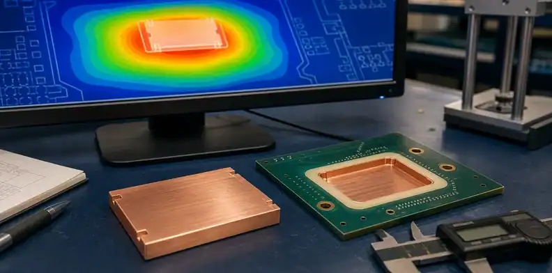
Review the cross-section behind the coin or inlay label
Use the cross-section to identify the insert’s exposed faces, connected layers and insulation boundaries. Match those features to the fabrication sequence before approving a drawing labelled “copper coin” or “copper inlay.”
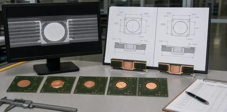
Illustrative drawing review: Two proposals use the same “copper inlay” description. Proposal A shows a solid insert extending through the board, with exposed upper and lower faces; the process note places insertion after the opening is machined in the laminated board. Proposal B shows an insert buried below an outer dielectric, with a separate component pad connected to it through specified plated vias; its process note places the insert in the lay-up. These are hypothetical constructions for reviewing drawings.
For A, check which exposed face contacts the component and which contacts the cooling assembly. Confirm the intended electrical connection and the method for securing the insert. For B, trace the component pad’s connection through the vias to the buried copper and identify the dielectric that separates it from nearby conductors. The external pad and the buried insert require separate feature definitions.
Suppose Proposal B’s assembly drawing also calls for soldering the device directly to an exposed insert face. That instruction conflicts with the covered insert in its section. Choose whether to expose the insert or attach the device to the surface pad, then revise the section and assembly drawing. Check that the layer data and build sequence agree. Record the approved construction in the drawing revision before CAM preparation; retain the coin or inlay label as a description of that defined feature.
Build a realistic dimensional tolerance chain
Finished coplanarity is the result of multiple dimensions, not just coin thickness. The chain can include core thickness, prepreg flow, cavity depth, coin thickness, copper foil and plating buildup, grinding or planarization removal, solder-mask thickness and final board thickness.
Separate functional tolerances from process targets. For example, a component may require a limited height difference between its solder pads and the exposed coin. That finished relationship is a functional requirement. The supplier may choose coin stock and planarization allowances that achieve it; those intermediate values should be shown in the approved manufacturing proposal.
Create a tolerance table:
| Relationship | Define on | Why it matters |
|---|---|---|
| Coin X-Y position to component land | fabrication/assembly datum drawing | Controls device-to-thermal-path alignment |
| Coin thickness and local board thickness | insert and board drawings | Establishes material available for planarization |
| Cavity-to-coin clearance | manufacturing proposal | Controls insertion, bonding and resin distribution |
| Exposed coin height to adjacent copper | finished board acceptance | Controls solder paste, package seating and interface material |
| Coin edge to internal conductors | layer artwork and section | Protects electrical clearance and lamination integrity |
| Finished board bow and local flatness | inspection plan | Prevents a locally correct insert in a distorted panel |
Overall board thickness selection still affects assembly and enclosure fit. Link the coin zone to the PCB board thickness decision rather than specifying the insert independently from the mechanical envelope.
When the supplier proposes a different insert size or grind allowance, require an updated tolerance calculation. A change that improves manufacturing yield can still move the exposed surface outside the assembly window.
Control bonding, resin flow and lamination
Bonding check: Accept the process only when resin distribution supports the coin without unacceptable voids, conductor displacement, or loss of dielectric clearance.
The insert must remain located while resin fills the intended interface and the multilayer stack consolidates. Too little flow can leave voids or incomplete support; uncontrolled flow can move the coin, contaminate an exposed surface, alter dielectric thickness or starve another region.
The lay-up review should identify:
- when the coin enters the build sequence;
- how it is retained or tooled during lamination;
- prepreg or bonding material around the insert;
- resin-flow paths and areas that must remain clear;
- pressure distribution over the metal discontinuity;
- expected movement and compensation;
- post-lamination machining or planarization.
Coin surface preparation also influences adhesion. The process may require cleaning and controlled roughening on bonded faces while preserving the finish of an exposed contact surface. The buyer should specify the functional surface condition and allow the qualified supplier to propose a compatible preparation route.
Asymmetric copper and a large local metal mass can affect heat transfer during lamination and panel flatness after cooling. Review panel orientation, copper balance and support tooling. Connect global distortion acceptance to the existing PCB bow and twist requirements while keeping local coin coplanarity as a separate measured result.
For first articles, ask for a section through the most difficult coin edge and a surface measurement across the exposed region. Those two views answer different questions: the section shows the hidden bond, while the surface map shows whether assembly can use the result.
Specify flatness and planarization at the surface
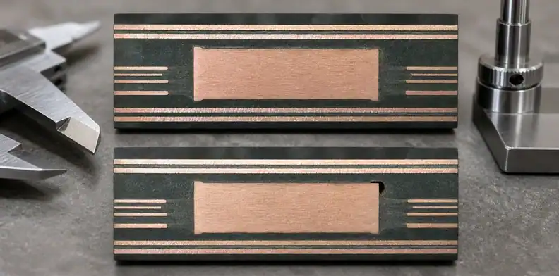
Planarization establishes the relationship between the coin and nearby copper after lamination and plating. A process that produces a smooth panel in one trial may remove too much coin, expose an interface, thin adjacent copper or vary across a larger production panel.
Define the measurement area and datum. “Coin must be flat” is ambiguous because it can refer to the coin surface itself, height relative to local laminate, height relative to component pads, or global panel flatness. State the maximum permitted step, the region over which it is measured and whether solder mask or surface finish is included.
The inspection method should fit the tolerance. Mechanical gauges may be adequate for a broad step; optical profilometry or another mapped measurement may be needed for a fine assembly interface. Require calibrated equipment and a report that identifies locations, not a single unlabeled number.
Review the effect of later processes:
- outer-layer copper plating can change adjacent pad height;
- surface finish adds a different deposit to copper and possibly the coin;
- solder mask can create another local step or keepout;
- final routing can release panel stress;
- baking or assembly heat can reveal a weak interface.
Coordinate the coin surface with the PCB tolerance stack-up review. The assembly drawing should use the finished values that matter to package seating and thermal-interface material, not nominal coin stock dimensions.
Prove the electrical and thermal path
Evidence check: Electrical continuity, dielectric isolation, and thermal contact answer different questions and need separate verification where each function is controlled.
Thermal performance depends on contact area, interface condition, copper path, coin geometry and boundary conditions. Copper conductivity alone does not prove that the built board meets the system objective. Define what evidence is practical for the design stage and what belongs to system validation.
At board level, useful evidence can include:
- dimensional confirmation of the heat path;
- cross-section of coin-to-copper and coin-to-dielectric interfaces;
- X-ray or another suitable method for hidden voids when validated for the geometry;
- continuity or resistance measurements when the coin is electrically connected;
- insulation testing when isolation is required;
- thermal test coupons or a product-level temperature study tied to stated conditions.
Do not accept an unqualified thermal conductivity value as a finished-board result. It may describe bulk copper rather than the complete interface. If suppliers provide simulation, compare material properties, contact assumptions, heat input and boundary conditions before comparing temperatures.
Electrical connection can be intentional, isolated or mixed by surface. Mark each interface. A coin tied to ground may need robust copper connection and plating; an isolated thermal insert needs controlled dielectric separation. The inspection plan should prove the selected condition without relying on visual inference.
Choose evidence and lot disposition
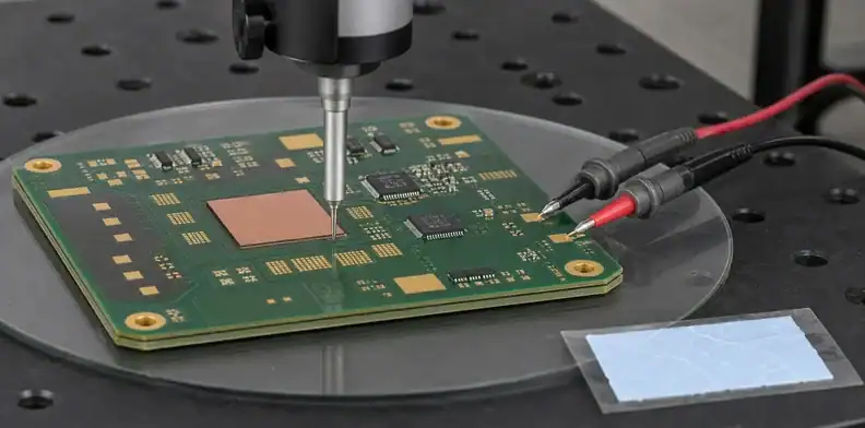
Evidence should be planned around failure modes. Surface measurement addresses coplanarity. Microsection addresses resin distribution, dielectric condition and hidden bonding. X-ray may reveal some void patterns. Electrical tests address connection or isolation. No single method proves all conditions.
For each first article or controlled lot, define:
- coin material and dimensional certificate;
- panel and coin traceability;
- insertion or lay-up inspection;
- post-lamination position and surface measurement;
- representative hidden-interface evidence;
- electrical and thermal checks required by function;
- response to a failed measurement.
Disposition rules should identify affected panels and related inserts. If one section shows a resin void, the response should determine whether it is local damage, systematic flow starvation or a tooling issue. Additional sections, process-record review or non-destructive inspection may be needed before the lot can be accepted.
Repairs require caution. Filling an exposed edge, grinding a high coin or adding local plating can change insulation, thickness, flatness and thermal behavior. Require engineering approval and a post-repair verification plan rather than accepting cosmetic correction.
Repeat production should retain the approved coin supplier or material specification, drawing revision, bonding process family, planarization method and evidence format. A purchase order that names only the finished PCB part number cannot control those variables.
Packaging and handling may need local protection when the coin is exposed above or level with the board surface. Abrasion, fingerprints, oxidation or contact with separators can change a thermal or solderable interface after final inspection. State whether the exposed surface receives a finish, protective film or dedicated tray feature, and require the final inspection record to precede controlled packing. Incoming inspection can then distinguish shipping damage from fabrication nonconformance.
Separate bare-board qualification from assembled-device evidence
Identify the specimen in each qualification report: a bare board, a soldered test assembly or the finished product with its cooling hardware. Follow the measured result to the interface being accepted. A board connection measurement and a device solder-joint measurement cover different parts of the construction.
The UIC AREA Consortium’s 2020 public copper-coin research abstract describes thermal cycling of T-shaped coin boards carrying QFN packages. It lists board circuitry, coin attachment epoxy, plated copper and solder joints or pads as examination targets. This published abstract identifies the study’s scope; it does not provide acceptance limits or lifetime results.
| Evidence supplied | What the report can support | What still needs evidence |
|---|---|---|
| Bare-board exposure, with identified continuity or insulation measurements and interface sections | The tested board connections, insulation boundaries and sampled interfaces under the stated exposure | Device solder joints and the cooling interfaces added during assembly |
| Thermally cycled assembly coupon, with monitored circuits and post-test failure analysis | The assembled interfaces represented by the coupon and covered by its measurements | Interfaces outside the monitored circuits; product heat transfer under operating load |
| Powered product test with recorded losses, temperatures and cooling conditions | The complete thermal path at the tested operating point | Durability under the required temperature or power-cycling exposure |
Illustrative document review: A supplier submits a bare-board cycling report that records stable resistance through the coin connection. The intended product mounts a QFN on that coin. Record the result under the board-connection acceptance item and keep the package-joint item open. Request assembly evidence for those joints. Define the coupon construction, monitored paths and failure-location analysis needed to close that gap. A product temperature measurement can be a separate requirement where the completed heat path is part of acceptance.
Keep the specimen revision beside its material stack, insert geometry, attachment process and assembly history. Record whether the test varies ambient temperature or device power, together with temperature limits, dwell or transfer times, cycle count and measurement intervals. Treat reflow exposure as an assembly-process check with its own conditions. If a report omits one of these details, identify the missing information and leave that acceptance item open until the evidence is supplied.
What Files Do You Need for a Copper Coin PCB Quote?
Send normal PCB fabrication outputs together with a controlled drawing of the coin interface. Gerbers and drill files alone leave the insert material, cavity fit and finished height undefined. In KiCad, export the normal manufacturing layers and drill data, then include the supplementary fabrication drawing in the same revision-controlled package; KiCad’s fabrication-output documentation covers the standard exports. Confirm separately that the quotation channel accepts a custom copper insert.
- Board data: Gerbers or agreed intelligent fabrication data, plated and non-plated drill files, board outline, stack-up and material specification.
- Coin and cavity drawing: dimensions, location datums, material and finish, plus a section showing the coin depth and its relationship to every affected layer.
- Finished interface: permitted coin-to-pad height difference, measurement region, exposed surfaces and solder-mask keepouts.
- Electrical and assembly requirements: connected nets or insulation boundaries, device contact area, attachment method and reflow requirements. Include BOM and placement files if assembly is requested.
- Order and acceptance scope: prototype and production quantities, drawing revision, required first-article measurements and any agreed cross-section, electrical or thermal checks.
| Controlled interface | Definition needed for quotation |
|---|---|
| Coin to cavity | Material, dimensions, datums, clearance and insertion stage |
| Coin to board surface | Finished height, coplanarity area, finish and measurement method |
| Coin to dielectric | Insulation boundary, bonding material and void evidence |
| Coin to component | Thermal contact area, assembly material and allowed surface condition |
Ask each supplier to return:
- proposed coin material, source and manufacturing route;
- build sequence and insertion stage;
- cavity and insert compensation assumptions;
- bonding material and resin-flow control approach;
- planned planarization and plating sequence;
- achievable local coplanarity tied to a measurement method;
- hidden-interface and surface evidence;
- thermal or electrical validation assumptions;
- first-article cost, recurring evidence and change-control conditions.
The quotation comparison should show assumptions beside price. Suppliers may use different coin architectures that cannot be compared from a single line item. Freeze the accepted construction in a named revision and require approval before changing the insert, cavity, bonding route or finishing process.
If the coin geometry is not finalized, mark that requirement as a design-review item instead of allowing an unrecorded CAM assumption. Ask for a proposed section, unresolved tolerances and the inspection scope before accepting the manufacturing route. A quoted board price and a validated product thermal result are separate deliverables.
To obtain a technical quotation, provide the thermal requirement, stack-up, component drawing, coin geometry, cavity definition, finished height relationship, assembly profile, evidence needs, and expected volume on the QueenEMS contact page. This package supports a fabrication answer instead of an estimate based on an undefined copper insert.
FAQ
Is a copper coin the same as a metal-core PCB?
No. A copper coin is a local insert integrated into selected board regions, while a metal-core PCB normally uses a continuous metal base as part of the board construction.
Should the coin be flush with the PCB surface?
Specify the finished height relationship required by assembly or thermal contact. Flush may be appropriate, but the datum, measurement area, surface finish and permitted step must be defined.
Can thermal vias replace an embedded copper coin?
Sometimes. Compare heat input, available area, board architecture, electrical isolation and system boundary conditions. The decision requires a thermal path assessment rather than a generic conductivity comparison.
What evidence finds voids around a copper coin?
Use a validated combination of representative cross-sections, suitable non-destructive inspection and process records. The appropriate method depends on coin geometry, surrounding materials and the size and location of relevant voids.
Sources
- IPC, IPC-2581C Generic Requirements table of contents
- IPC, Challenges of Manufacturing with Printed Circuit Board Cavities
Written by the QueenEMS Engineering Team
Upload your files today · Free DFM check before production · Ship worldwide
Get your PCB prototypes in as fast as 24 hours. We handle FR4, Rogers, and hybrid boards up to 40 layers in volume production, with advanced builds subject to engineering review — free prototypes for 2–4 layer FR-4 boards, no minimum order.
Just upload your Gerber + BOM — we source every part, assemble, and inspect (AOI + X‑Ray) so you don't have to chase suppliers. Boards ship in as fast as 24 hours.