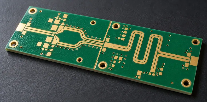
Quick Answer: Choose RF PCB solder mask coverage from the finished line’s electrical requirements and protection needs, rather than a blanket rule to expose every RF trace. Include the actual mask layer in the model and compare representative constructions with declared finish, geometry and measurement boundaries. If removing mask also changes the surface finish, the result compares complete builds; it does not isolate the mask’s contribution.
A prototype report says the open line has less loss. Before changing the production artwork, ask what else changed: the exposed metal, the line dimensions, or the launches used to measure it. Those details decide what the comparison can support.
Why does solder mask change RF microstrip loss and impedance?
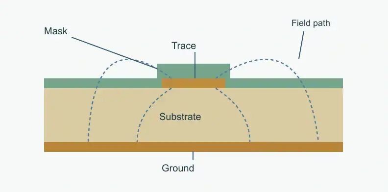
Microstrip fields extend through the substrate and the space above the conductor. A mask layer replaces some of that air with a dielectric, changing the effective dielectric environment and adding dielectric loss. The resulting impedance and transmission response depend on the actual formulation, finished thickness and coverage, together with the line's geometry.
Rogers' discussion of solder mask on RF and microwave boards addresses that electrical effect alongside the protection a mask provides. It describes increased effective Dk and dielectric loss when mask is added to microstrip or grounded coplanar lines on low-loss laminates. The coating therefore belongs in the circuit model when it is present on the finished line.
Do not assign the laminate's Dk and Df to the mask. They describe different materials, and neither alone describes the whole transmission path. Keep dielectric, conductor and radiation effects separate when discussing the source of loss. A lower laminate Df does not remove the need to account for the other construction members.
This guide concerns outer-layer RF transmission lines. A buried stripline does not have the same local air-and-mask environment, so an outer-line comparison should not be applied to it without a separate analysis.
When should solder mask be removed from RF microstrip lines?
Consider removing mask where its modeled or measured electrical effect leaves insufficient margin against the project's loss or impedance requirements. Keep it when the finished construction satisfies those requirements and its protection is needed. Review the exposed finish and assembly consequences before approving a change; operating frequency alone does not settle the decision.
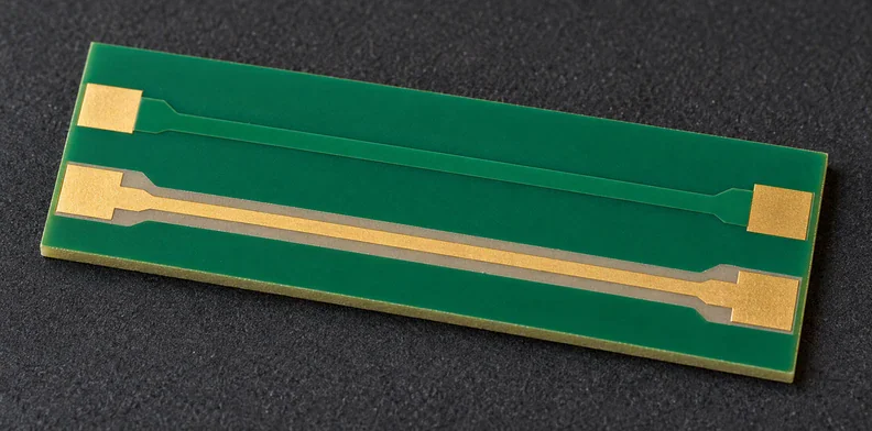
Start with the released model. If it assumes an uncovered line but the artwork covers that line, resolve the discrepancy before comparing results. Conversely, removing mask from a design that was modeled and qualified with it changes the construction being accepted. Neither change is automatically an improvement.
Protection remains a design requirement even when electrical performance favors an opening. Identify how the exposed conductor will be finished, handled and kept suitable for the product's assembly and service environment. Retain any mask needed around soldered components unless its removal has been reviewed with the assembly owner.
Use the solder mask opening requirements guide for pad definition and registration. Those geometric rules do not determine how much electrical change an RF line can tolerate. There is no universal frequency cutoff or mask-clearance number in this article.
How does surface finish confound a solder mask comparison?
An opened line may receive a different finish from a covered conductor, depending on the fabrication route. That creates another variable in the comparison. If finish type, coverage or condition changes alongside mask coverage, the measured difference cannot be assigned to mask alone. It describes the two finished constructions under the stated measurement conditions.
Rogers' millimeter-wave transmission-line discussion identifies copper roughness and plated finish among the contributors to conductor loss. That supports recording the actual metal system; it does not provide a fixed finish penalty for every RF frequency, geometry or plating route.
Distinguish two legitimate questions. To choose between production builds, compare each complete construction as it will be supplied. To isolate a mask effect, the experiment needs a feasible pair with matched finish and other relevant variables. The second task is harder, and the fabricator and appointed test owner must confirm whether that pair can actually be made and evaluated.
For example, “covered copper versus exposed finished copper” can inform a build choice. Labeling the same result “loss caused only by mask” would claim more than the comparison establishes. Preserve the construction descriptions with the report instead of identifying samples only by their colors.
How should buyers build a controlled mask comparison?
Declare whether the comparison isolates mask coverage or selects between complete builds. For isolation, match the other relevant variables and record any unavoidable differences. Identify the mask product, finished coating and metal condition, then agree the measurement boundary with the test owner. Confirm the proposed specimens are feasible before ordering them as a controlled pair.
This proposed planning matrix lists what a buyer needs to resolve. It is not a test standard, a universal coupon design or an offer of a QueenEMS measurement service.
| Variable | Comparison record |
|---|---|
| Line geometry and length | Same drawing revision; record actual dimensions and any differences |
| Laminate and copper | Product, dielectric thickness and copper construction held consistent |
| Mask coverage | Declared variable: covered or open over the identified line region |
| Mask material and processing | Product, finished thickness, coverage boundary and cure condition |
| Surface finish | Type, coverage and condition; flag a change as a second variable |
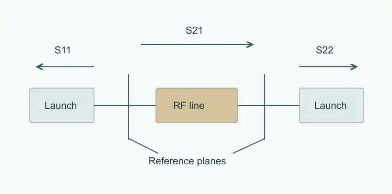
| Launches and reference planes | Same boundary and fixture treatment, with any exceptions explained |
| Electrical observations | S21, S11 and S22 over the agreed frequency band; impedance evidence as specified |
| Measurement responsibility | Named test owner, method, specimen condition and raw data record |
For a mask-isolation pair, cure history and other processing differences also need review. Removing a coating after fabrication may introduce changes beyond the intended variable. Ask the parties designing the comparison to identify those differences rather than assuming a post-processed sample represents a production mask-off route.
How do you compare insertion loss from measured S21?
At the same frequency and reference planes, convert each transmission magnitude to insertion loss using a declared convention. Compare both results with the project limit, then examine reflections and the full required band. A difference in measured transmission does not by itself establish dielectric loss, dissipated power or a change attributable only to solder mask.
For this example, IL = −20 log10|S21|, where |S21| is the linear transmission magnitude; a reading of 20 log10|S21| = −0.80 dB therefore corresponds to 0.80 dB insertion loss. The following readings and limit are invented solely to demonstrate the arithmetic. They are not QueenEMS measurements, recommended limits or per-inch values.
| Construction at f0 | Transmission magnitude, dB | Insertion loss | Hypothetical maximum: 0.90 dB |
|---|---|---|---|
| A | −0.80 dB | 0.80 dB | Pass at f0 |
| B | −1.05 dB | 1.05 dB | Fail at f0 |
Do not identify A as “mask off” until the specimen record supplies that fact. Even then, inspect its finish and geometry before attributing the difference. Check S11 and S22 because reflected energy affects transmission, and retain the fixture or de-embedding definition so launch changes are visible.
Preserve the original complex data across the specified band. An impedance requirement also needs its own stated method and result; a passing S21 point does not prove it. Routine board inspection does not imply that either RF measurement was performed.
What should an RF PCB fabrication RFQ specify about mask and finish?
Identify masked and open RF regions in the fabrication data, with the proposed stackup and finish coverage. State which mask properties the electrical model assumes and which substitutions need approval. Name the RF test owner and any requested comparison specimens. Keep unresolved material, manufacturing and measurement questions visible in the quotation instead of relying on defaults.
Send the mask layer with the copper data, not an isolated screenshot. Attach the relevant model assumptions and construction revision. If performance depends on a named mask product or finished thickness, identify that dependency for feasibility review; do not assume the fabricator stocks it or guarantees the modeled result.
Use the separate guide to qualifying an RF PCB fabricator for the broader supplier decision. Here the quotation should resolve the proposed construction and list any exclusions. The customer's chosen RF test owner defines the measurement method and evidence needed for acceptance.
Frequently Asked Questions
Does solder mask color matter for RF performance?
Color alone is not a selection basis. Obtain the specific product’s electrical data and model its finished thickness and coverage. A familiar color does not establish the same formulation or RF response.
If the mask-off sample has a different finish, can I credit the loss change to the mask?
No. You can compare the complete constructions for a build decision, but isolating the mask effect requires a feasible matched-finish comparison with the other relevant variables controlled.
Is lower insertion loss the same as lower heat in the line?
No. Transmission also depends on reflection and the stated measurement boundary. A power-dissipation or thermal assessment requires its own inputs and analysis; S21 alone does not establish how much heat the line dissipates.
Will standard PCB inspection confirm the RF loss of my mask construction?
No. Routine inspection does not imply RF S-parameter testing. Appoint a test owner and agree the method, specimen and data package before relying on an RF acceptance claim.
Send your released files for a quote and free DFM review.
Send Gerber, stackup and the solder-mask drawing for review. Identify the RF areas, proposed mask extent and performance evidence required by your design.
For an assembled RF board, add the BOM and the mask-sensitive component locations. Agree the assembly inspection scope separately from RF validation.