
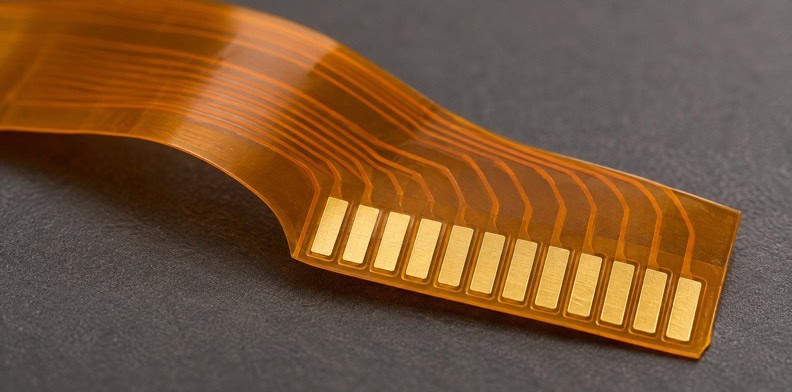
Quick Answer: PCB coverlay is a protective insulating covering, commonly a polyimide film with adhesive, laminated over flexible circuitry. For fabrication, define the copper that must remain exposed, identify each side’s coverlay data, and state whether openings may be combined. Keep coverlay termination, rigid-area windows and stiffener outlines separately identifiable.
An opening that looks correct in the design viewer may leave too little usable contact area after fabrication. The order package should describe the finished exposure the product needs, so the manufacturer can review the pattern and raise changes before the board is built. This guide focuses on that drawing and quotation task.
What is coverlay on a flex PCB?
Film-based coverlay commonly consists of polyimide film and an adhesive layer that bonds it over the flexible circuit. It insulates and protects conductors while leaving selected features exposed through openings. The material and opening pattern are part of the finished board construction, so they need identifiable fabrication data and requirements.
The adhesive bonds the film and fills around the circuit features during lamination. An exposed pad, contact finger or test location therefore needs more than a note saying that the board uses coverlay. Its required access must survive the selected material and fabrication process.
Different film and adhesive constructions affect the finished stack. Ask for a proposal against your bending, exposure and electrical requirements. Detailed adhesive selection belongs in the flex PCB adhesive guide; the task here is to make the opening and its function clear.
The film and adhesive perform related but distinct jobs. The film provides the insulating covering; the adhesive attaches it to the circuit and occupies space around the copper features. A drawing that names only the film does not fully identify that bonded construction. When a material change is proposed, review both parts rather than assuming the visible film name describes the entire stack.
Coverlay openings are deliberate interruptions in that protection. They may expose a soldering area, a mating contact or another feature that needs access. The surrounding copper can still require insulation. This is why a visually neat opening is not enough to define the finished requirement: the designer must identify both the area that needs exposure and any nearby conductor that must remain covered.
When is coverlay chosen instead of flexible solder mask?
Film coverlay is commonly considered for flexible regions that need substantial bending or repeated movement, while flexible solder mask can help define finer features in suitable areas. Choose by the complete construction and use conditions. Do not treat either material as a universal replacement for the other across the entire board.
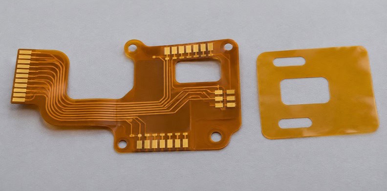
Epec’s coverlay and solder mask discussion describes differences between sheet-based coverlay openings and photo-defined mask features. It also describes designs that use the materials in different regions. The examples support choosing the protection region by region.
If fine-pitch pad access makes the coverlay pattern difficult, ask which opening or material arrangement the fabricator proposes. The design owner should review what copper would be exposed and where the protective materials meet. A finer pattern is useful only when the resulting construction also fits the board’s mechanical duty.
The manufacturing distinction helps explain the choice. A sheet of film needs openings formed in it, and the remaining pieces must survive handling and bonding. A photo-defined coating uses a different patterning approach. Epec describes how this affects small openings and the narrow webs between them. A rigid-board solder mask pattern therefore should not be assumed to transfer unchanged into film coverlay.
Define where bending occurs and whether the board moves during service or is formed during installation. Then identify the regions containing fine-pitch features. That information lets the fabricator assess a film, mask or regional combination against the actual use. A generic instruction to substitute flexible mask wherever coverlay is difficult leaves the mechanical requirement unanswered, even if the pad pattern becomes easier to form.
Why can the finished opening differ from the drawn opening?
The cut pattern, its registration to copper and adhesive movement during lamination all affect the finished exposed area. Registration variation can shift an opening, while adhesive flowing into it can reduce clear access. State the exposure your design needs, then ask the fabricator to explain how its proposed pattern achieves it.
PCBGOGO’s explanation of coverlay squeeze-out describes adhesive flow around openings and its effect on the available opening. Some flow helps the bond and encapsulation; its presence alone does not establish a defect. The relevant acceptance question is whether the agreed finished feature remains usable.
A solder pad may need access for attachment, while a contact finger needs a defined mating area. A test opening has another purpose. Record those functions instead of applying one unexplained expansion to every opening in the layout.
Ask which drawing note defines the finished result and which file defines the proposed cut. If those two definitions conflict, obtain a marked-up response. A supplier’s suggested enlargement or offset is a proposal until the designer approves it; it should not silently replace the functional requirement.
Separate positional variation from a reduction in clear opening. In a hypothetical rectangular contact window, a shifted pattern can cover more of one edge while exposing more copper at the opposite edge. Adhesive entering the window can instead reduce the available clear area around the feature. The same drawing outline can therefore raise different questions about the finished contact. Ask the supplier to address the required usable area, not only the nominal cut size.
Making the opening larger may recover contact access but expose a neighboring trace or remove a narrow protective web. Review the overlay of copper and proposed coverlay together. The relevant tradeoff is visible there: the contact needs usable exposure while the adjacent circuitry may need continuous insulation. Neither a universal opening expansion nor a universal prohibition on squeeze-out resolves that design-specific requirement.
How should coverlay openings be defined in the design files?
Identify the coverlay pattern for each board side, link it to the copper features it exposes, and state the function and required finished access for critical openings. Use clear file names, orientation and revisions. Distinguish coverlay data from solder mask data so the manufacturer does not have to infer their intended roles.
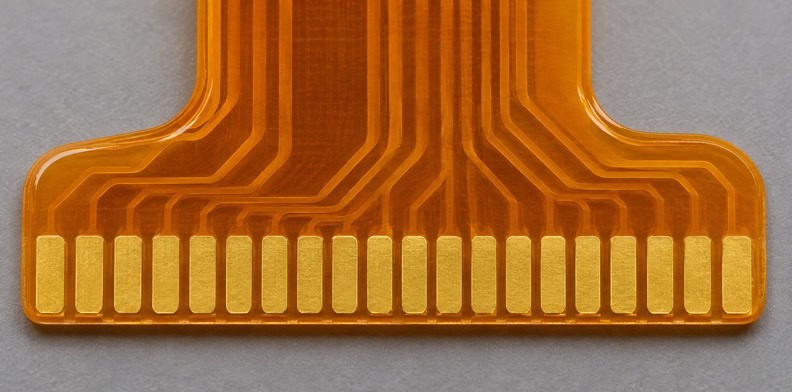
The following editorial opening-intent table can accompany the fabrication drawing. It is a working checklist, not an industry form or a statement of QueenEMS’s process. Fill the fields with project information rather than copying a supplier’s generic tolerance into the order.
| Opening field | Define in the package | Ask the supplier to return |
|---|---|---|
| Feature and purpose | Pad, contact, test location or other named function | Any access concern for that feature |
| Side and pattern | Board side, coverlay data layer and orientation | Confirmation of the interpreted pattern |
| Finished exposure | Copper area that must remain accessible | Pattern and process assumptions used to achieve it |
| Grouping | Individual openings or permission to propose a group | The extra copper exposed by a proposed group |
| Boundary and revision | Nearby transition or support edge and document revision | Marked exceptions needing design approval |
For a mirrored bottom-side view, make the orientation explicit. Keep the feature identifiers consistent between the mechanical drawing and layout. A visually plausible opening on the wrong side can survive a quick review if the file names and viewing convention are unclear.
For a practical file review, select a recognizable feature near one end of the board and find it in the copper, coverlay and outline views. Check its side and orientation in each. Repeat this at the critical exposed area rather than relying on a symmetrical outline, which can hide a mirrored interpretation. Keep the review image as an explanatory aid; issue the controlled pattern data that the manufacturer will actually use.
Clarify what a drawn shape means. Does it identify an opening to cut, an area to keep covered, or a mechanical reference used only for review? A file named “coverlay” does not settle that question by itself. Include a legend and state any permitted supplier compensation separately from the finished exposure requirement. If the manufacturer returns compensated data for approval, identify that returned revision in the order package.
When can openings be ganged, and who approves it?
A fabricator may propose one larger opening over several pads when separate openings leave fragile film features or are difficult to register. The design owner should approve that proposal because it changes what is exposed between the pads. Show whether grouping is allowed, restricted or still awaiting review in the fabrication package.
The Epec discussion describes combining openings to avoid fragile webs and detached film features. That is a manufacturability option rather than permission to expose every nearby conductor. Compare the proposed opening with the copper and the function of the finished area.
Consider an illustrative row of contact pads with a signal trace passing between pad groups under coverlay. Individual openings expose the contacts while covering the trace. A proposed single opening across the group could also expose that trace. Overlay the proposed opening on the copper layer and have the designer decide whether the added exposure is acceptable. Checking only that every pad remains visible would miss the change.
Return the decision to the controlled pattern and drawing. An email approval without an updated file can leave the buyer and manufacturer working from different definitions on a repeat order. Identify which revision replaces the earlier pattern and whether any other openings remain unchanged.
Review the pieces of film left between and around openings. A long narrow web and an isolated island are different shapes, but both raise handling or bonding questions that a copper-only view can hide. Ask the fabricator to mark the features it considers difficult in the proposed material. This keeps the discussion tied to actual geometry rather than assigning a universal minimum web size from another supplier’s process.
For the contact-row example, the designer could retain separate windows, approve a grouped opening where the extra exposure is acceptable, or revise the local layout. Those are alternative design decisions, not interchangeable CAM edits. The fabricator can explain the manufacturability concern and proposed pattern; the design owner determines which exposed conductors and protective boundaries the product can accept.
Where should coverlay stop on a rigid-flex board?
Define the coverlay termination separately from the rigid-material opening and any stiffener outline. Their locations serve different purposes even when they meet near the same transition. Show their intended relationship in a view or detail, then have the fabricator identify any construction change that needs the design owner’s approval.
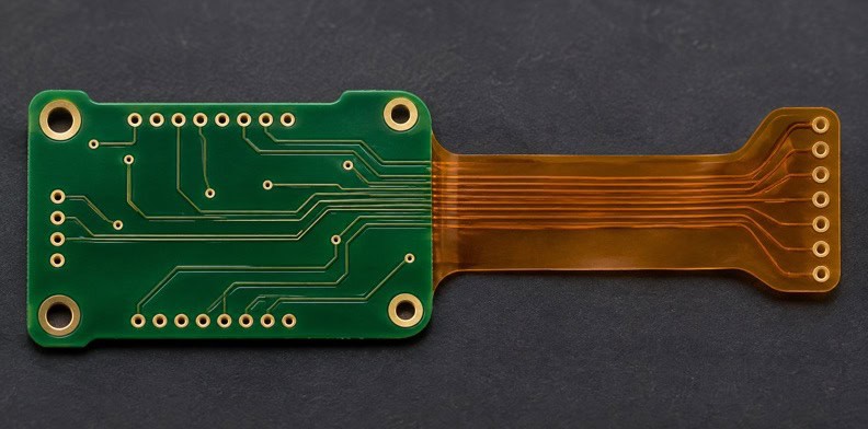
PCBWay’s article “What is Flex PCB Coverlay?” describes a common arrangement using coverlay on flexible portions and solder mask on rigid portions. Some designs instead use coverlay across the rigid-flex board. For that arrangement, show which rigid-area features remain covered and which need windows. These are construction choices to confirm with the fabricator, not a universal layout rule.
Name the arrangement your design intends, show where coverlay ends relative to the rigid edge, and ask the manufacturer to confirm it or mark an alternative. The drawing should let a reviewer follow the protective surface from the flex span into the rigid region.
A regional stackup explains which materials are present; the boundary drawing explains where they end. Use the same region identifiers in both. A coverlay edge should not be assumed to coincide with a rigid edge merely because the drawing uses one line for both.
Check how the plan view and section view describe the same interface. The plan locates the termination along the board; the section shows its relationship to the other materials. If one view suggests coverlay continues into the rigid region and the other shows it ending before the rigid edge, ask for resolution before quotation approval.
For a supported connector or component area, the flex PCB stiffener requirements guide addresses the support’s function, side and finished thickness. Keep those requirements distinct from the coverlay pattern.
Before issuing the order, check three separate boundaries: the coverlay termination, the rigid-material window over the flex, and the support outline where used. For each, record its drawing reference, related region and open supplier question.
Frequently Asked Questions
Is coverlay the same as solder mask?
They both protect circuitry, but film coverlay and flexible solder mask use different material and patterning approaches. Confirm which protection applies to each region rather than treating their data layers as interchangeable.
Can the supplier change my coverlay openings?
The supplier can propose changes during DFM. Review the resulting exposed copper and have the responsible design owner approve the revised pattern before manufacture.
Is adhesive squeeze-out a defect?
Some flow is expected during coverlay bonding. Judge the finished result against the agreed exposure, insulation and workmanship requirements rather than treating any visible flow as an automatic failure.
What coverlay thickness should I specify?
It depends on the copper features, finished construction and bending or electrical requirements. State the functional requirements and review the fabricator’s proposed film and adhesive construction without assuming a universal thickness.
Send your released files for a quote and free DFM review.
Send Gerber, coverlay patterns and the fabrication drawing for review. Mark finished exposed areas, board side and critical opening boundaries.
For assembly, add the BOM and show which exposed areas receive components or connections. Confirm placement and inspection needs against the approved coverlay revision.