
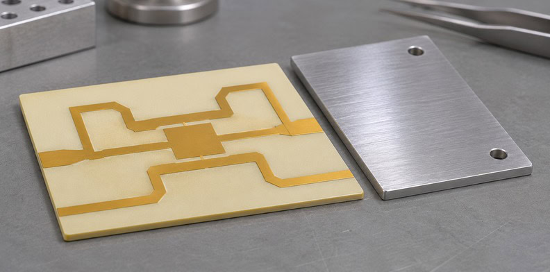
Quick Answer: Define a metal-backed RF PCB through its electrical, thermal and mechanical interfaces before ordering. Identify the RF reference copper, the bond’s required electrical behavior, the metal spreader and its housing contacts separately. A thermally conductive bond may also conduct current, so the drawing must show where electrical connection or isolation is intended.
A metal spreader can occupy the same physical area as an RF circuit without having the same electrical job as its reference plane. A quotation that specifies only laminate and backplate metal leaves their relationship unresolved. The fabrication package should connect the RF stack, bond area and machined member to the housing drawing, so purchasing orders the construction engineering intended.
How is a bonded metal backing different from a metal core?
A bonded metal backing is a metal member attached to an outside face of the circuit construction. An internal metal core occupies a position within the board structure. Show the actual section rather than relying on either name, because that location determines which materials and electrical connections lie between the circuit and metal.
In the arrangement considered here, the circuit construction has its own copper layers and dielectric materials. A bond joins its back surface to a metal spreader. The spreader may also have pockets, fastener holes or surfaces that locate against a module housing. Each of those features belongs to the supplied physical construction, even when the Gerber artwork only depicts the circuit.
Begin with a view through a critical RF trace. Identify the signal conductor and the copper plane used as its electrical reference. Continue through the remaining materials until reaching the metal backing. If a material or gap is omitted from that view, a reader cannot tell whether the proposed backing changes the intended electromagnetic geometry.
Then draw a section through a mounting feature or a thermal contact. It may cross a different sequence of materials from the RF trace. A single simplified stack illustration can miss a pocket where the metal approaches the circuit or a fastener that creates an electrical connection.
The existing discussion of hybrid PCB lamination addresses compatibility within a mixed laminate stack. Use it for that separate internal construction problem. The added question here is how the external metal member and its bond relate to the completed circuit and housing.
These drawing recommendations describe the intended product. The manufacturing sequence remains a proposal to review with the fabricator; a section drawing should not quietly prescribe a bonding process that has never been confirmed.
What do bond-film and handling data tell you?
They identify properties and processing considerations for a particular material system; they do not establish every bonded board’s performance. Check whether a proposed film conducts electricity as well as heat, and review its compatibility with the laminate and subsequent operations. Material identity belongs in the construction definition before process details are approved.
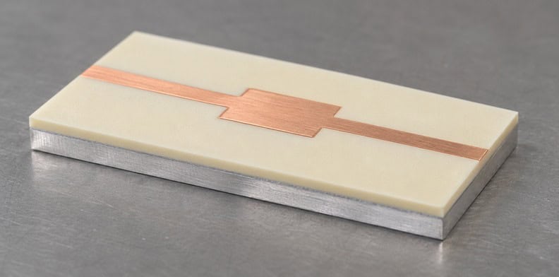
For a specific example, Rogers describes COOLSPAN TECA as a silver-filled epoxy adhesive film that is both thermally and electrically conductive, with uses including bonding high-power circuit boards and metal backplanes. That example demonstrates why “thermal adhesive” is insufficient wording when the drawing also requires electrical isolation.
The Rogers CuClad fabrication guide, pages 2–3, discusses handling of soft PTFE-based laminates and metal plates, where handling damage such as scratches or dents can affect later processing. It also describes adhesive selection in relation to electrical performance, flow and bonding temperature, with the bonding cycle determined by the chosen adhesive system. These are material-specific fabrication considerations, not a universal RF bonding recipe.
| Published information | What it supports | What still needs project definition |
|---|---|---|
| A film conducts heat and electricity | Electrical behavior must be checked explicitly | Which surfaces and nets may connect |
| Adhesives have different flow and bonding requirements | Material selection and process compatibility are linked | Approved bond extent and finished construction |
| Laminate and metal surfaces need careful handling | Surface condition can affect subsequent work | Protected areas and applicable finished requirements |
This table is an editorial interpretation of the named materials, not a list of QueenEMS stock or qualified processes. If a different film or laminate is proposed, evaluate that system’s own current documentation. Keep a supplier’s product description distinct from evidence that the complete circuit, bond and backing meet the order requirements.
Is the backing part of the RF return path or isolated from it?
The circuit designer must define that electrical role, and the construction drawing must preserve it. A backing may have an intended connection to circuit ground, chassis or another reference, or may require isolation. Show the permitted paths through the bond, fasteners and exposed contacts rather than inferring them from the metal’s thermal purpose.
RF return current is associated with the transmission-line geometry and its reference structure. Calling the backing “ground” does not identify the copper plane used by a particular trace. Label that reference copper in the stack and show how it connects, if required, to the added metal.
Consider an illustrative circuit with a continuous reference copper plane above a bond layer and spreader. The reference plane’s location is part of the RF geometry. The spreader’s electrical relationship to that plane is a separate interface decision. The drawing should identify both, including any intended connection around the perimeter or through mounting hardware.
Where the backing must remain isolated, inspect the entire path through the assembly. An insulating bond area does not resolve an unreviewed screw or exposed edge contact. Conversely, a required connection needs a defined contact location and surface condition; it should not depend on incidental pressure between unqualified faces.
Separate a required electrical connection from a claim about its RF behavior. An end-to-end continuity check can establish a conducting path under its test conditions, but it does not describe the path’s geometry at the operating frequency. The circuit designer should identify any frequency-dependent requirement that the construction must preserve, including relevant connector and housing contacts.
The controlled-impedance manufacturing guide covers the line geometry and associated fabrication requirements. Reference those requirements by layer and feature in this package. Do not replace them with a general statement that a metal spreader improves RF performance.
Record an unresolved electrical relationship as an engineering decision before quotation acceptance. A fabricator can assess the proposed construction, but purchasing should not choose a conductive or insulating bond solely because one alternative is available sooner.
Which features must match the mating housing?
Match the backing’s locating surfaces, pockets, holes, connector clearances and contact faces to the actual housing datums. Define their relationship to the circuit, including any bond contribution to finished height. A correct circuit outline does not establish that a machined spreader will locate or clamp correctly in its enclosure.
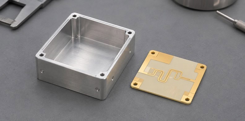
Use the surface that locates the product
A datum is the reference used to locate or measure another feature. Choose the housing-related face or feature that controls the assembly, then show how the circuit and backing locate from it. Dimensioning the board and metal from unrelated references can leave their individual drawings readable while their relative position remains undefined.
For example, a connector opening can clear the nominal circuit outline yet interfere with a spreader pocket or with the board’s finished vertical position. A section through the connector and housing shoulder should show the relevant surfaces together. The required clearance comes from that assembly design and its agreed tolerances.
| Mating feature | Relationship to show | Engineering decision |
|---|---|---|
| Housing seating face | Backing face and finished circuit height | Which face controls location |
| Fastener hole | Housing datum, metal and circuit clearance | Mechanical and electrical function |
| Pocket or recess | Depth reference and local circuit section | Clearance or contact requirement |
| Thermal contact area | Defined mating surface and interface layer | Applicable flatness and contact condition |
Define the finished condition
Identify the measurement condition for each finished-dimensional requirement. Where acceptance depends on a fixture, agree that setup before making its result an order requirement.
Set bond and surface acceptance against the actual application and agreed specification. Avoid copying a general void percentage or flatness figure from an unrelated construction. The necessary requirement should describe a feature whose effect the engineering owner can explain.
How should the cross-section assign every interface?
Assign each interface an electrical function, a thermal function and a mechanical relationship, then connect those requirements to identified section views. Include the RF reference copper, bond, spreader and chassis contact. This lets each engineering owner review the same construction instead of approving disconnected circuit, adhesive and metal drawings.
Use the following matrix as an editorial planning aid. It identifies questions to resolve, not default acceptance limits. Add the drawing reference and responsible engineering owner for each row in your own project copy.
| Element or interface | Electrical requirement | Thermal requirement | Mechanical definition |
|---|---|---|---|
| RF reference copper | Named reference and net relationship | Its role in the intended heat path | Position in the circuit stack |
| Circuit-to-metal bond | Connection or isolation intent | Specified bond system and contact extent | Finished bond contribution and boundaries |
| Metal spreader | Ground, chassis or isolated role | Required heat-transfer interfaces | Material, pockets, datums and finished dimensions |
| Spreader-to-housing contact | Permitted contact and fastener paths | External interface arrangement | Seating area and fastening condition |
For an illustrative annotation, mark a section through an RF trace as A–A and a section through a mounting hole as B–B. In A–A, identify the trace, reference copper, remaining dielectric, bond and spreader in their physical order. In B–B, identify which materials the fastener passes through and where it may make contact.
If a pocket changes that order locally, add a detail view tied to the pocket outline. The material sequence at the trace cannot serve as a substitute for the sequence beneath a recessed component or around a screw.
Give the bond outline its own identity where it differs from the board profile. A drawing that shows only the circuit and metal perimeter leaves the bond’s edge and openings undefined. Keep permitted contact areas and areas that must remain clear distinguishable, including the face from which each view is read.
When a bond opening surrounds a hole, reference both outlines to the same feature location. A metal-part drawing and a circuit export can each show the correct hole while leaving the intervening adhesive opening ambiguous. The coordinated detail should let the reviewer follow that opening through the supplied construction without inferring its shape from a generic bonding note.
Which engineering decisions need a fabricator response?
Request a response to unresolved construction decisions: the proposed bond system, achievable finished geometry, protection of contact surfaces and the method for checking critical interfaces. Evaluate each proposal against the electrical and mechanical intent already defined. A proposed bond material may address the thermal requirement while changing electrical continuity.
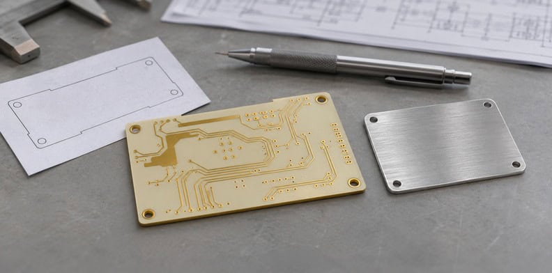
A machining proposal may preserve a pocket’s dimensions while using a different locating face. Ask for the consequence of each proposal in the coordinated drawing, so its acceptance does not create a contradiction elsewhere in the package.
Where a finished feature cannot be checked directly, agree how its relevant characteristic will be demonstrated and which party performs that work. The method should match the feature being accepted; a general inspection method should not be treated as proof of every hidden interface.
Also distinguish acceptance of the separate parts from acceptance after bonding. A circuit can meet its own outline requirement while its position on the spreader is wrong. Identify which dimensions describe the finished combined item and which records address the incoming parts. This gives the supplier a concrete basis for proposing an inspection sequence without turning the order into a factory work instruction.
QueenEMS (Queenpcb Limited) has more than 10 years of experience and offers UL and IPC Class 3 support. A particular RF laminate, bond film, metal backing and machining combination still requires project review. Include the desired quantity and material constraints with the construction files so feasibility and quotation scope can be considered together.
Close a proposed change by revising the affected drawing or material note before production authorization. Keep the accepted electrical paths, mechanical datums and bond boundaries in that released definition for repeat orders.
Frequently Asked Questions
Does adding metal backing change PCB impedance?
It can affect the electromagnetic construction, depending on the reference structure and intervening materials. Identify the intended reference copper and the backing’s electrical relationship to it, then review the actual geometry. A backing specification alone cannot establish the impedance of a particular line or replace the design’s controlled-impedance requirements.
Can the backing serve as ground?
Only if the electrical design and completed construction define that role. Identify where it connects, the mating surfaces and any isolation required elsewhere. A thermally conductive bond may also conduct electricity, while mechanical fasteners can create additional contact paths. Review all of those paths together.
Is solder attachment equivalent to an adhesive-film bond?
Treat a change in attachment method as a construction proposal requiring review. The electrical behavior, finished interface and compatibility with later operations need to satisfy the same defined requirements. Do not accept a replacement method merely because both approaches join the circuit and metal physically.
Who should define flatness for a metal-backed RF board?
The mechanical design owner should define the functional requirement against the mating assembly, with the fabricator confirming the proposed construction and measurement method. State the surface, datum and condition being checked, including whether the requirement applies before bonding, after bonding or in the assembled fixture.
Send your released files for a quote and free DFM review.
Send Gerber, RF stackup and the backing-metal drawing for review. Identify interface, attachment and inspection requirements for the quotation. Ask us to confirm project feasibility.
If the backed RF board needs assembly, show fitted parts and backing-related access limits. Agree who supplies and attaches each item in the quoted scope.