
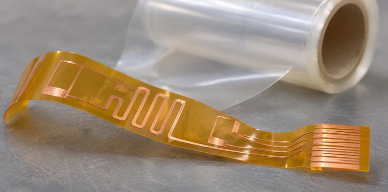
Quick Answer: LCP PCB manufacturing requirements should identify the film, copper foil and complete bonding construction, together with the finished holes, registration and electrical geometry. “LCP” names a material family rather than a complete build. Supply the intended design dimensions and require a fabricator proposal for material compatibility and process compensation before releasing the board.
An LCP circuit uses liquid crystal polymer as part of its insulating construction. A material-family label leaves open which film and copper laminate the buyer intends, how additional layers join and what the finished circuit must satisfy. For a high-frequency flex or another special-material board, the order needs that construction identity alongside the copper pattern. The following drawing recommendations help turn the material choice into a reviewable manufacturing request.
Why is LCP alone insufficient for a PCB specification?
An LCP PCB specification must identify the actual insulating film, copper and joining layers because those materials form the finished circuit together. Naming the polymer does not specify their grades, dimensions or interfaces. Start with a section of the intended construction and identify every material the fabricator is expected to retain or propose.
Separate three objects in that section. Film is the polymer material. Copper-clad laminate combines an insulating material with copper foil. A completed circuit may add patterned copper, plated connections, bonding layers, protective layers or local supports. Information about the film alone does not define all those additional elements.
Check that the material document describes the object being purchased. A property sheet for an LCP molding compound does not identify a circuit laminate, even when both use the same polymer-family abbreviation. The drawing’s material reference should lead the reviewer to the film or laminate designation used in the proposed board construction.
For a single circuit region, show which copper face is used and where a protective layer begins or ends. For a multilayer request, identify the named copper levels and the material between them. If part of the construction is undecided, describe the required function and mark it for a supplier proposal rather than leaving an unexplained blank.
Also identify what the product asks the circuit to do mechanically. A fixed folded interconnect, a repeatedly moving flex and a supported RF circuit pose different design questions. Provide the relevant geometry and use condition without assigning a universal bend-life claim to the polymer name.
The broader PCB materials guide covers material-family selection. Here the task begins after LCP has become a candidate: translate that choice into a specific construction that can be evaluated for fabrication.
A useful first review is to ask whether two manufacturers could interpret the drawing as two different physical stacks. If one could quote a film-based construction and another could add an unspecified bonding layer while both claim compliance, the material definition needs another decision before price comparison.
What does one supplier’s LCP material data show?
It shows properties and construction examples for named grades under stated conditions, rather than universal LCP limits. Read the material designation, test method and document revision with each value. Keep melting behavior, dielectric properties and demonstrated laminate construction separate from the finished-board requirements the supplier must confirm for your project.
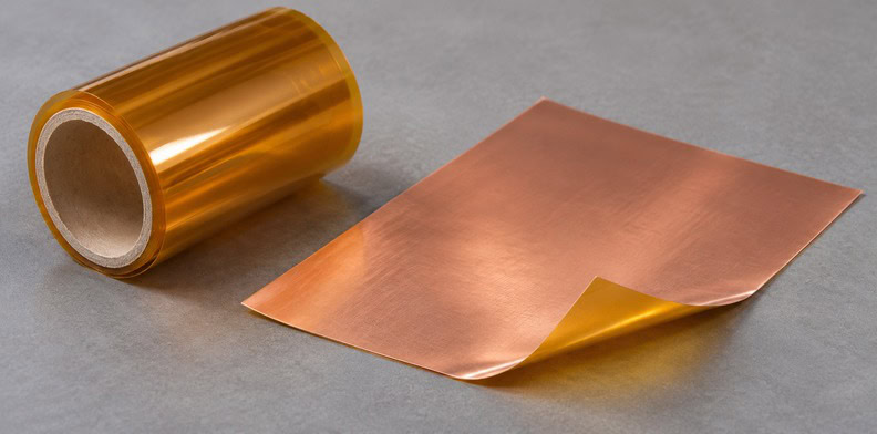
Kuraray describes VECSTAR as a thermoplastic LCP film used as a circuit-board substrate material, with low water absorption and high-frequency electrical characteristics. Its June 2019 flexible copper-clad laminate brochure gives the following examples. The brochure identifies its data as typical values that are not guaranteed; current designations and supply conditions still need confirmation.
| Brochure item | Q series example | F series example | How to use the information |
|---|---|---|---|
| LCP film thickness options | 25, 50 and 100 µm | 25, 50 and 100 µm | Identify the specific laminate designation |
| Copper in the standard-material table | 12 µm ED foil | 12 µm ED foil | Do not assume a different foil from the polymer name |
| Film melting temperature, DSC method | 310°C | 280°C | Material behavior, not a PCB press or service-temperature instruction |
ED means electrodeposited copper. The example demonstrates that a named LCP construction can include a specific foil type and thickness. It does not establish which copper treatment or finished conductor thickness is appropriate for another design.
The brochure also illustrates a bonded multilayer arrangement and an all-LCP arrangement. Treat those as identified material-system examples, not interchangeable interpretations of an incomplete order. Its conditional hole-processing examples likewise cannot be converted into a universal drill diameter, preparation chemistry or guaranteed finished limit.
Use the example to ask better construction questions. The manufacturer should confirm the actual material system proposed for the released drawing; neither the brochure’s melting temperature nor a generic material-property table supplies that manufacturing approval.
Which LCP PCB manufacturing requirements belong in the material callout?
Call out the supplier designation, film and copper construction, bonding layers, protective materials and the status of any proposed alternatives. Identify which dimensions refer to incoming material and which refer to the finished circuit. This makes the order specific enough to review without turning it into a fabricator’s process instruction.
Use this identity table as an editorial planning aid. The entries are fields for your approved design, not a suggested universal stack. A material option awaiting review should be visible in the confirmation column until engineering accepts it.
| Element | Definition to retain | Confirmation needed |
|---|---|---|
| Copper-clad laminate | Supplier, full designation and required revision | Proposed material identity and availability |
| LCP film | Grade, thickness and relevant orientation | Relationship to the quoted laminate |
| Copper foil | Type, treatment and starting thickness where controlled | Finished conductor requirement and proposed allowance |
| Joining layers | Named bonding material or an identified proposal | Compatibility and finished stack contribution |
| Protective layer | Material and opening boundaries | Local section and finished geometry |
| Local support | Position, side and thickness requirement | Mating feature and attachment definition |
Distinguish a supplier’s description of a copper-clad laminate from the complete multilayer stack. A statement about how copper attaches to the base film does not define how the finished circuit’s other layers will join. Show those joining layers explicitly wherever they are present.
If the design permits a different bonding approach, state which functional requirements remain fixed. An alternative might change the finished dielectric spacing or material at an exposed edge. Ask for those construction consequences in the proposal, then approve the resulting stack rather than accepting a familiar material-family name.
Keep the region-specific definition readable. A connector tail with a local support can have a different finished thickness from the free circuit span even though the underlying film is continuous. Identify both sections and their boundaries so the supplier can review the contact geometry.
What should the drawing say about holes and registration?
Identify the function, finished size and location requirements of each hole type, then relate those features to named layers and mechanical datums. Registration requirements describe how features must align in the finished circuit. The fabricator should propose the processing route against that definition rather than infer it from a generic LCP note.
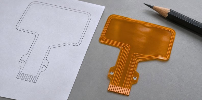
A plated connection, a tooling feature and an unplated mounting hole serve different purposes. Keep those categories distinct in the drill documentation. For a connection between particular copper levels, show which levels it joins and where it sits in the local material section.
Define registration at the features that need it. A copper pad aligned to a hole, a protective-layer opening aligned to a contact and a circuit outline aligned to a connector support are separate relationships. A single undifferentiated “alignment” note does not tell the reviewer which relationship controls the design.
For an RF interconnect, use a detail view where a connector contact, opening and local support meet. Show the contact side and the locating features. The finished circuit must fit that interface; nominal film thickness by itself does not determine the completed connector-tail thickness.
Keep the viewing direction explicit when features on opposite faces overlap. A support drawn from the underside can appear mirrored relative to the contact artwork unless both views use a stated reference. Key the detail to the same profile and locating features so a reviewer can determine which surface each material or opening occupies.
Where film orientation is controlled, identify it consistently with the feature coordinates and the material documentation. This gives the fabricator a defined reference when proposing material placement and dimensional compensation. Do not infer an orientation requirement from the way an exported drawing happens to fit the page.
Leave the choice of drilling, preparation and plating conditions with the proposed manufacturing route. Ask how the finished connection and alignment requirements will be addressed, and identify any unconfirmed feature before the order is released. Material literature showing a successful demonstration does not qualify every combination of layer count, hole geometry and joining material.
Who compensates artwork for dimensional change?
The fabricator should establish process compensation from the approved material construction and its manufacturing controls. Supply the intended finished design dimensions without adding an assumed shrink factor. If any data have already been scaled, identify that transformation explicitly so the supplier can avoid applying another correction to the same features.
Compensation is the deliberate adjustment of production artwork to obtain the specified finished geometry after processing. It is different from changing the design’s required dimensions. The native design, exported artwork, mechanical drawing and supplier’s production data should retain a traceable relationship.
Connect a drawing request to the finished features
Consider an illustrative LCP circuit with an RF trace, a plated connection near one end and a locally supported connector tail. The request identifies the intended outline and contact positions, the named copper levels, the connection’s endpoints and the support boundary. Engineering also provides the required relationship between the connector contacts and locating features.
The drawing asks the fabricator to propose a construction and explain any necessary production compensation. It does not tell purchasing to enlarge the Gerber files by an internet percentage. Once the proposed stack and finished requirements are approved, the fabricator can relate its compensated production data to that controlled design.
Keep a record of which file is design data and which is a supplier-generated manufacturing derivative. A production file returned for information should not silently replace the native design master. Otherwise a later export may incorporate a prior compensation and invite a second adjustment.
For joining-layer questions, the related flex PCB adhesive guide explains the broader distinction between adhesive materials and their functions. In this request, retain the particular joining layer in the local section so its dimensional contribution remains visible.
How should impedance targets and finished acceptance be stated?
State the controlled line, its reference structure, the target and permitted tolerance, and the finished construction to which those requirements apply. Give the operating context needed to assess the material proposal. A film’s dielectric data supports material selection but does not establish the impedance or loss of a manufactured transmission line.
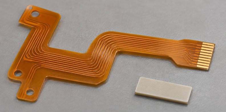
Identify the signal layer and its reference conductor in the section view. Include the joining and protective materials that are part of that geometry. A proposed change to one of those layers may need electrical review even when the copper pattern remains unchanged.
Distinguish the design requirement from the method used to evaluate it. If a coupon or another verification arrangement is required, agree its relationship to the circuit and the applicable measurement conditions. The supplier’s general test menu does not decide the project’s required electrical checks.
For a material property, retain the reported method, frequency, direction and condition with the value used in the design. For a finished-circuit requirement, state the feature and method being accepted. Keeping those two levels distinct helps engineering review a laminate alternative without treating a datasheet number as a board test result.
QueenEMS (Queenpcb Limited) has more than 10 years of experience. General company capabilities do not establish an LCP material or process combination, so submit the specific construction for project confirmation.
Before ordering, resolve the proposed material identity, local geometry and verification scope together. The released files should describe the same finished circuit that the quotation assumes.
Frequently Asked Questions
Is LCP better than polyimide for every flex circuit?
No material family is a universal choice. Compare the actual electrical, mechanical and environmental requirements with a specific proposed construction. A fixed RF interconnect and a repeatedly moving flex can require different evaluations. Generic property comparisons do not establish the suitability or manufacturability of the complete circuit.
Can an LCP PCB include other insulating materials?
A proposed construction may include joining or protective materials in addition to the named LCP film. Identify each material and its location rather than assuming the whole circuit contains only LCP. Any mixed construction needs review against the required electrical geometry, mechanical use and manufacturing compatibility.
Should I specify a particular copper roughness?
Specify the copper characteristics the electrical and manufacturing design requires, using a defined material designation and relevant measurement basis. Do not infer surface condition solely from a label such as rolled or electrodeposited foil. Review the proposed foil, treatment and completed conductor together where loss or bonding performance is sensitive to them.
What does typical mean in an LCP datasheet?
A typical value describes the supplier’s reported material data under its stated conditions; it is not automatically a guaranteed purchase limit. Check the current material documentation and identify any property that must become a controlled order requirement. Finished-board dimensions and electrical acceptance still need their own definitions.
Send your released files for a quote and free DFM review.
Send the proposed LCP construction, Gerber and fabrication drawing for review. Identify the material designation and ask us to confirm project feasibility.
If the proposed LCP board requires assembly, add the BOM and placement drawing. Confirm the supported construction and assembly conditions before ordering.