Quick Answer: A copper invar copper PCB order needs a defined role for the composite metal and a complete material callout, including supplier designation, thickness ratio, total thickness and surface condition. Show its position and electrical relationships in the construction drawing. The expansion behavior of a metal sheet alone does not establish the flatness or reliability of the completed board.
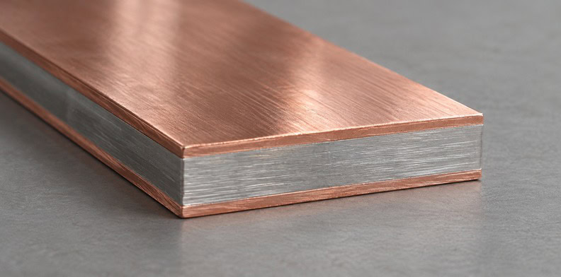
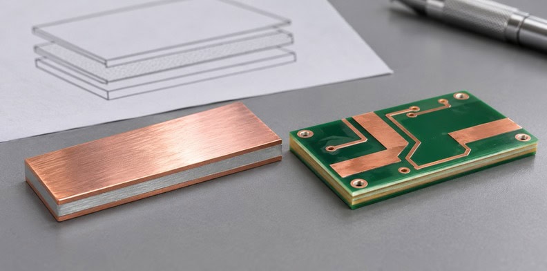
Copper-Invar-Copper, also called CIC, is a metallic composite with copper on both sides of an Invar layer. It can be considered when a PCB construction needs a particular combination of expansion behavior and conduction. The purchasing question is how that sheet becomes a defined member of the board. A drawing must explain its job, its interfaces and the properties that matter to the application before a fabricator can assess the proposed build.
What job can copper-invar-copper do in a PCB?
Define whether the composite is intended as a conducting plane, a member that constrains expansion, or a separate heat-spreading part associated with the board. Each role leads to different connection, location and interface requirements. A material name alone does not tell the fabricator which of those functions the design requires.
CTE means coefficient of thermal expansion: it describes dimensional change with temperature over a stated interval. When expansion control is the reason for selecting a composite, identify the dimension, direction and temperature interval that matter to the design. “Low CTE” without that context is an incomplete requirement.
The copper faces and central Invar belong to one composite metal sheet. They are not the same object as a finished multilayer board containing dielectric materials and additional circuit copper. Keep the material’s own description separate from the board section into which it may be incorporated.
A conducting-plane proposal needs an electrical identity and intended connections. A constraining member needs a defined place and extent in the stack. A separate spreader needs its own attachment and mating-surface definition. If the same member performs more than one job, show those functions together so they can be reviewed for compatibility.
For an illustrative order, call the proposed composite member M1 in the stack drawing. A note saying only “M1: CIC” leaves its electrical role unresolved. A more useful request identifies M1’s material callout, its intended net or isolation condition, and the dimensions controlling its location. The fabricator can then assess a specific construction rather than infer a purpose from the material name.
What does supplier data show about thickness ratios?
Different copper-to-Invar thickness ratios have different published expansion and conduction properties, so the ratio must be part of the material identity. Read each value with its temperature interval and direction. A sheet property is useful for comparing candidate materials, but it is not a measured result for the completed PCB.
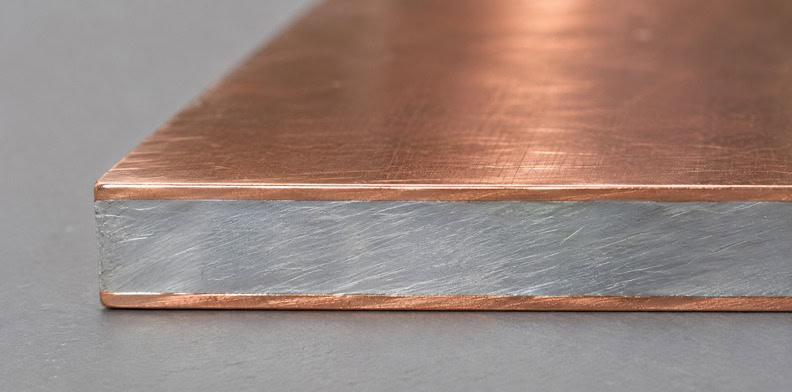
The Engineered Materials Solutions CIC datasheet, carrying a 2014 printed date, describes a roll-bonded metallic composite and reports the following data for two thickness ratios. These are values from that dated supplier sheet, not current purchase guarantees, QueenEMS measurements or finished-board acceptance limits. Confirm the applicable current material specification before ordering.
| Cu/Invar/Cu thickness ratio | CTE, −55 to +125°C | Thermal conductivity, in-plane / through-thickness | Electrical conductivity |
|---|---|---|---|
| 12.5 / 75 / 12.5 | 2.4–5.6 ppm/°C | 110 / 20 W/(m·K) | 25% IACS |
| 20 / 60 / 20 | 3.6–6.8 ppm/°C | 167 / 20 W/(m·K) | 40% IACS |
The ratios describe the relative thicknesses of the three metal layers, not the chemical composition of an alloy. The thermal-conductivity entries convert the sheet’s W/(cm·°C) units to W/(m·K). In-plane means along the sheet; through-thickness means across it. IACS is a reference scale for electrical conductivity, not a current rating for a particular trace or plane.
Read the tradeoff across the row rather than selecting the largest conduction value. The sheet reports different CTE ranges as well as different electrical and in-plane thermal conductivity for the two ratios. The through-thickness figure also differs from the in-plane figure; substituting one direction for the other would change the material assumption.
These data support asking for a specific ratio and the properties relevant to its intended role. They do not specify a completed board’s thermal resistance, warpage, current capacity or service life, and the sheet’s material-processing information is not a PCB lamination instruction.
How does the chosen role change connection and isolation requirements?
A conducting role needs named connections to the composite, while an isolated or constraining role needs defined separations from circuit features. Show which holes, edges and contacts may touch the metal member. The drawing should distinguish intentional connections from features that merely pass near or through its position in the stack.
Begin with the electrical purpose assigned to M1. If it is a ground or power member, identify the intended net and the locations where the design expects contact. If it has a mechanical purpose without an intended circuit connection, define that condition explicitly rather than leaving its electrical status to incidental contact.
A hole crossing the member’s location requires a section showing the intended connection or isolation. The finished hole’s coordinate and size do not fully describe how the conductive sheet relates to its wall. Keep the metal outline, any clearance boundary and the named circuit layers distinguishable.
If the design calls for a break in a conducting region, define which part of the composite that break concerns. A gap drawn in a copper face does not, by itself, specify a discontinuity through the entire metal member. Show the intended electrical separation in section and request a construction proposal for that outcome.
The related metal-core hole-isolation guide explains that broader topology problem. Its example constructions are not automatically the manufacturing route for a CIC design. Use the underlying distinction between intentional contact and isolation, then request review of this particular composite and stack.
Consider the exposed board edge as well as drilled features. A metal member reaching the perimeter has a different contact condition from one that terminates inside the surrounding construction. Show the required extent and any relevant edge treatment or insulation in the drawing.
For a separate spreader, trace the connection through its attachment and fastening arrangement instead. A statement that the part is “outside the PCB” does not resolve whether it contacts ground, chassis or an isolated surface. Keep that electrical definition with the mechanical drawing used for the supplied part.
What must a complete CIC material callout include?
Include the supplier and designation, copper/Invar/copper thickness ratio, total thickness, material condition, surface treatment and intended function. Where a property is controlled, state its direction and temperature interval. The callout should identify the material the engineering design intends, with any alternative held for a separate approval decision.
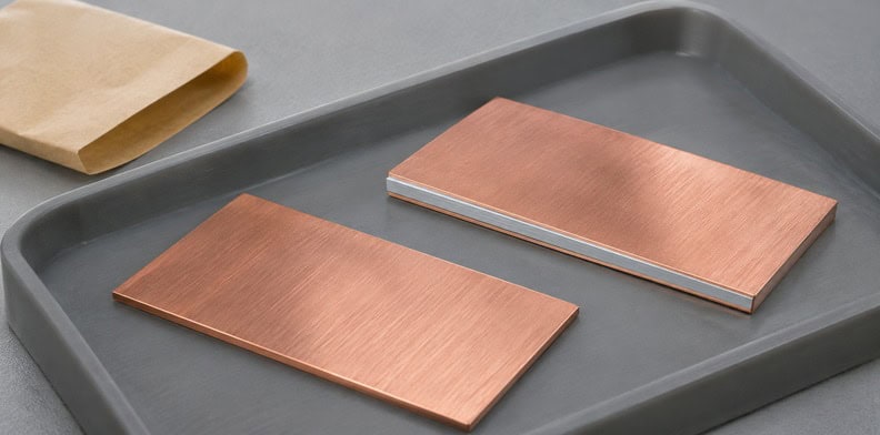
The following callout template is an editorial planning aid. Replace each field with the project’s approved value or mark it as a proposal awaiting confirmation. A blank field should not be interpreted as unrestricted material selection.
| Callout field | What the drawing should identify | Reason for keeping it explicit |
|---|---|---|
| Material identity | Supplier, designation and governing document | Separates the proposed product from a generic composite name |
| Geometry | Thickness ratio, total thickness and member outline | Connects the material proportions to the actual member |
| Condition and surfaces | Temper of the composite and treatment of each relevant face | Defines the material presented to the joining interface |
| Function | Plane, constraining member, spreader or combined role | Connects material selection to the design task |
| Controlled properties | Required characteristic, direction and temperature interval | Prevents an unrelated datasheet value being treated as the requirement |
CCI Eurolam’s CIC material page describes treated and untreated supply options and copper or copper/zinc surface treatments used in relation to laminate bonding. That is a material-source example, not evidence that every treatment is suitable for the proposed PCB stack or available through QueenEMS.
Identify the treated face where the design depends on it. “Treated material” without a face or interface reference can leave the reviewer uncertain about which surface joins the dielectric or contacts another part. Relate the note to the section view and any supplied material documentation.
If a supplier proposes a different ratio, condition or treatment, retain the original callout as the comparison baseline. Review the changed material and its construction consequences before incorporating it into the released drawing.
How should the stack drawing present the composite for review?
Show the composite’s named position, outline and interfaces within the complete construction, then add sections through its critical contacts and clearances. Keep its material thickness separate from the finished board thickness. The drawing should let the reviewer trace where the member exists and how it relates to surrounding dielectric and copper layers.
Use the existing PCB stack-up design guide for the general layer-table framework. Add the composite member’s identity without renaming the circuit layers in a way that obscures their relationship to the fabrication data.
State whether a layer count refers to circuit copper or to named material members. The three constituent layers in one composite sheet should not be counted as three separately patterned routing layers without an explicit design definition. Keep each actual circuit-layer name tied to its exported artwork and describe the composite through its material callout.
This role-to-drawing matrix is an editorial planning aid, not a qualified construction list. A proposed role requires confirmation against the actual materials, geometry and manufacturing route.
| Intended role | Drawing information | Question for fabrication review |
|---|---|---|
| Conducting plane | Net identity, intended contacts and isolated features | How will the defined electrical relationships be formed and checked? |
| Expansion-constraining member | Stack location, extent and adjoining layers | How does the proposed construction meet the dimensional requirement? |
| Separate spreader | Mating surfaces, attachment and finished dimensions | How are the part and its interfaces supplied and accepted? |
| Combined function | All relevant electrical and mechanical requirements | Does meeting one role conflict with another? |
For an illustrative stack review, mark M1 in the layer table and show its outline on a separate mechanical layer. A section through a mounting hole identifies whether it contacts M1. A second section through the free board area shows the adjoining dielectric and the member’s position. Matching identifiers connect the local details to the full construction.
If M1 stops short of an edge or pocket, dimension that boundary from an identified datum. A material symbol in a stack table supplies no plan-view extent. The fabricator needs both views to assess the finished geometry and any proposed construction changes.
Why does low material CTE not guarantee flatness or life?
The completed board combines the composite with dielectric materials, circuit copper, joining interfaces and mechanical constraints. Its dimensional behavior therefore depends on the complete construction and conditions, rather than one sheet property alone. Define the finished characteristic that matters and review how the proposed stack will be evaluated against it.
Flatness is a geometric condition of a part or assembly under a defined measurement setup. CTE describes dimensional response over a temperature interval. The two concepts are related through the product’s construction, but a low material CTE number does not state the board’s acceptable shape before or after assembly.
If the design needs dimensional stability at a mounting interface, identify that interface and its operating conditions. If it needs compatibility with another member’s expansion, identify the relevant direction and temperature interval. Those requirements give engineering a basis for evaluating the complete proposal.
Keep the measurement condition with the result being requested. A room-temperature dimension on a free board and a dimension taken while the board is constrained in an assembly describe different conditions. Engineering should decide which condition represents the functional requirement, then agree a practical evaluation with the party responsible for the finished item.
Review symmetry and material distribution as construction questions rather than applying a blanket rule that adding a low-expansion sheet prevents distortion. Also separate a prototype result from a repeat production qualification. Any environmental or assembly evaluation should use the agreed construction and document the characteristic being assessed.
QueenEMS (Queenpcb Limited) has more than 10 years of experience and offers UL and IPC Class 3 support. Those general company facts do not qualify a particular CIC material, stack or joining route. Send the defined composite construction for project confirmation, including the quantity and any material constraints that affect the manufacturing request.
Frequently Asked Questions
Is copper-invar-copper the same as a copper coin?
No. Copper-invar-copper is a composite metal sheet with copper faces and an Invar layer, while a copper coin describes a localized copper insert in a particular board construction. Specify the actual member and intended function instead of treating the terms as interchangeable material options.
Can a CIC member carry electrical current?
It is a conducting metallic composite, but the suitability of a particular plane or connection depends on its material, geometry and electrical requirements. A published electrical-conductivity value is not an ampere rating. Define the intended connections and operating requirement for engineering and fabrication review.
Will adding CIC make the PCB heavier?
Assess the actual construction rather than the material name alone. The composite’s total thickness and outline, any material it replaces and the rest of the stack determine the change in mass. Request the relevant material and geometry information if assembly weight is a controlled design requirement.
Which copper/Invar/copper ratio should I choose?
Choose against the required expansion and conduction behavior, using current supplier data for a specific designation. Retain the temperature interval and property direction with that comparison. Then review the complete board construction; the ratio that suits a standalone sheet does not automatically establish the best finished PCB stack.
Send your released files for a quote and free DFM review.
Send the proposed CIC stackup, Gerber and construction drawing for review. Identify material evidence and ask us to confirm the requested build.
For assembly on the proposed CIC construction, identify fitted parts and mechanical interfaces. Request confirmation of project feasibility and quoted scope.