
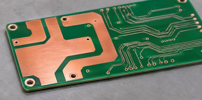
Quick Answer: Define local copper thickness zones on one PCB layer with a zone outline, finished conductor thickness, height reference and transition requirements. Show the surface condition needed by pads, contacts and protective coatings in section views. Submit that definition for a fabricator feasibility review; the drawing specifies the required outcome rather than establishing that a particular manufacturing route is available.
A power conductor and fine signal traces may impose different requirements on the same design. Before requesting a special local-thickness construction, decide whether placing those functions on separate copper levels would satisfy the product. If the design needs them on one level, a single copper-weight note cannot explain the intended geometry. The request needs a plan view showing each zone and sections explaining its thickness and surface position.
When should heavy copper go on separate layers instead?
Consider separate power and signal layers when the design can meet its electrical, thermal and mechanical requirements without different local thicknesses on one level. Request local zones only where the product needs that geometry. This keeps a special fabrication requirement tied to a defined function rather than a preference for heavier copper.
Start by identifying the reason for local thickness. It may concern a conductor’s cross-section, an external contact, a component interface or a restriction on where power can be routed. State the required function in the design request. The fabricator needs that context to explain whether a proposed alternative still addresses the problem.
If separate layers are acceptable, each layer can have its own defined finished-copper requirement. The heavy-copper RFQ guide addresses that per-layer schedule. Such a schedule does not, by itself, define multiple local thicknesses on one layer; it describes a different construction decision.
| Design decision | Definition needed | Question to resolve first |
|---|---|---|
| Different power and signal layers | Finished-copper requirement for each named layer | Can routing and interconnection satisfy the product? |
| Local zones on one layer | Zone outline, thickness, height reference and transitions | Why is this local geometry required? |
| Supplier-proposed alternative | Changed construction and its functional consequences | Does it preserve the requirement that led to the request? |
This is an editorial decision aid, not a menu of qualified processes. If the design depends on local geometry, retain the requirement during feasibility review and ask for an explicit response. A generic heavy-copper quotation cannot establish whether the requested local feature is included.
Keep a rejected alternative with the engineering reason for rejecting it. That prevents a later cost review from reintroducing separate layers or a different interface without recognizing which product constraint the local zone was meant to satisfy.
How do copper thickness, height and transition differ?
Thickness describes the conductor’s dimension through its metal; height describes a surface’s position relative to a stated datum; a transition identifies where the local geometry changes. Define all three when they affect the product. A thicker conductor does not, by its thickness callout alone, specify the finished position of its top surface.
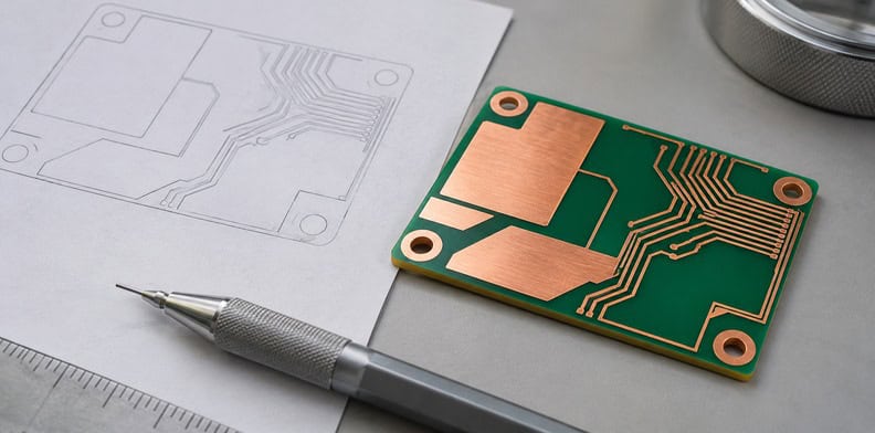
A datum is the reference from which a height or position is measured. It might be a defined laminate surface, a mechanical seating face or another design-controlled reference. Name it in the section view. “Height above board” leaves open which board surface the reviewer should use.
Consider two illustrative drawing outcomes. One request permits the top of a local power region to stand above adjacent signal copper. Another requires the relevant contact surfaces to finish at a common level. These are statements of required geometry, subject to fabricator confirmation; they do not describe methods for making either outcome.
In the first request, identify where the step is permitted and which nearby features must clear it. In the second, identify which surfaces must share the common level and what dimensional relationship controls that requirement. Neither drawing should leave the fabricator to infer the intended surface position from a copper-weight label.
Also distinguish metal thickness from a complete finished section that includes a coating or surface finish. A contact’s working height may concern the final contact face, while a conductor requirement concerns copper. State the object being measured so a correct reading of one does not become an incorrect assumption about the other.
The transition needs its own plan-view location and local section. The region boundary can affect adjacent features even when the copper remains electrically continuous across it.
How do you draw local copper thickness zones for review?
Give each zone a stable identifier and a defined outline on a named layer, then connect it to a finished-thickness and surface-height requirement in section. Keep the zone map aligned with the circuit coordinates and revision. Mark undecided dimensions as proposals for review instead of allowing a visual highlight to stand in for a specification.
The following table is an editorial template for a project copy. It contains fields to complete, not numerical capability limits. Attach the zone outline data and the corresponding section references so each row identifies a real location.
| Zone-map field | Required definition | What the reviewer can determine |
|---|---|---|
| Layer and zone ID | Named circuit level and unique zone label | Which physical conductors the request concerns |
| Plan-view extent | Outline data or coordinates tied to the board datum | Where the requirement begins and ends |
| Finished conductor thickness | Required value and dimensional basis | Which metal section must satisfy the design |
| Height and surface condition | Reference face and permitted step or common-level requirement | How the zone relates to adjacent features |
| Transition detail | Section reference and affected feature boundaries | Which local interfaces need review |
| Function and tolerance owner | Reason for the zone and responsible engineering decision | Which proposed changes require approval |
For an illustrative request, label a proposed power region P and the neighboring signal region S on the same circuit level. The plan view identifies P’s outline. A section crossing P–S defines the conductor thickness in each region and the permitted relationship between their top surfaces. A separate detail locates any contact or component affected by that relationship.
Keep an outline supplied for manufacturing definition distinguishable from circuit copper artwork. A colored shape in a PDF can explain intent, but the reviewer also needs an unambiguous boundary tied to the released coordinates. State which file controls if the illustrative view and machine-readable outline disagree.
As an illustrative completed row: zone P on layer L1; outline from the controlled zone-outline file at the current revision; finished conductor thickness per drawing note 4; height referenced to datum A, the laminate surface beneath S, with a step above S permitted; transition detail D-1; function: supply path to the output connector, owned by the power-stage engineer. Each entry points to a controlled note, so the row cannot drift from the drawing.
What should be defined at thick-to-thin transitions?
Define the transition’s location, permitted surface relationship and the nearby features whose spacing or coating depends on it. Show where pads, contacts and protective-layer boundaries lie relative to the change. The fabricator should assess those relationships against a proposed route rather than apply an unspecified local-thickness interpretation to the artwork.
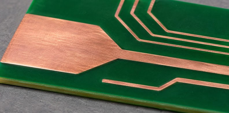
The end of a zone is not necessarily the same boundary as a component pad or mask opening. Name each boundary in a local detail. If the transition may occupy an area rather than an exact line, identify the permitted area and which features it must avoid.
Follow the electrical conductor across the boundary. The required conducting path, connection and clearance must remain identifiable in the proposed finished section. A top view alone cannot explain a vertical step that changes the space available beneath a component or alongside a contact.
For a protective coating, identify the surface it must cover and any area that must remain exposed. Ask how the proposed finished geometry relates to that requirement. Avoid assigning a universal coating thickness or clearance to every local step; the requirement should come from the actual construction and use.
Apply the same discipline to legend placement. A readable marking has a location and surface, and it should not be the only drawing feature that defines a copper zone. Keep electrical and dimensional boundaries in controlled manufacturing data even if a legend also identifies the region.
The broader heavy-copper design guide covers layout considerations for thick conductors. This local detail adds a different requirement: where one specified section changes to another on the same circuit level. Ask the fabricator to mark any proposed relocation or geometric change against that detail before accepting the quotation.
How do pads, contacts and plated holes interact with local thickness?
Review each affected pad, contact and hole against its local finished section. Copper thickness, contact height and hole-wall copper are different characteristics, even when they meet at the same feature. State the required relationship and ask the fabricator to explain how its proposed construction addresses each characteristic without assuming that one measurement proves the others.
A MacDermid technical paper hosted by IPC evaluates plated copper at hole-wall and surface locations separately when discussing microdistribution. That supports distinguishing those measurement locations. It does not establish a selective-height manufacturing route or provide acceptance limits for the local-zone request described here.
Specify the hole’s function and its required connection to the local conductor. The surface copper next to a hole does not, by itself, state the copper condition along its wall. If the design requires a particular wall characteristic, retain that requirement separately in the hole definition.
Check the surface used by the next operation
A component supported by pads in different zones needs a defined seating relationship. Identify which pads are affected and show the final surfaces the assembly uses. Any implications for solder deposition or assembly fixturing should be reviewed with the assembly owner against the proposed construction.
A pressure contact likewise needs a defined working face and its position relative to the locating features. A conductor’s nominal thickness is not a complete contact-height requirement. State whether the applicable dimension includes a surface finish, and identify the measurement reference.
Where a hole and transition meet, add a section through both rather than reusing a section through an uninterrupted zone. That view lets the fabricator identify a potential conflict and propose a geometry change for review. These are engineering questions about the required result, not instructions for plating chemistry or production setup.
How should you judge a fabricator’s response to the map?
Compare the proposed section, zone extents, finished surface relationships and verification approach with the requirement attached to each zone. Accept a route only after its deviations and unresolved features have engineering dispositions. A response that changes the required geometry is an alternative proposal, even if it uses the same general heavy-copper description.
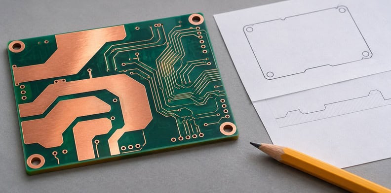
The illustrative P–S request is explicitly subject to fabricator confirmation. A useful response identifies the proposed finished geometry in P, S and their transition, then addresses the pads, contacts and holes tied to those sections. It should distinguish a confirmed feature from a feature that still needs a trial or a different design.
If the response proposes separate power and signal layers, check it against the rejected-alternative record from the first decision before engineering accepts the change.
Agree the characteristic and location to be checked for each critical requirement. Conductor thickness, step height and contact coplanarity need corresponding measurement definitions. A generic sample photograph cannot establish every dimension in the zone map.
QueenEMS (Queenpcb Limited) has more than 10 years of experience. This request concerns a specific local-copper geometry that requires project feasibility confirmation; no general layer-count or inspection statement establishes that construction. Include the quantity and relevant material constraints with the proposed outcome so the manufacturing review addresses the intended order.
Retain the approved section and any accepted deviations in the released drawing. If the proposed route cannot satisfy the required geometry, keep the item unresolved and review the design alternative before authorizing fabrication.
Frequently Asked Questions
Are local zones the same as different copper weights on separate layers?
No. A per-layer schedule assigns a copper requirement to each named circuit level. A local-zone request assigns different requirements to defined regions on one level, including their transitions and surface relationship. State which construction the design needs rather than using a general mixed-copper description.
Does defining a local zone select a manufacturing process?
No. The zone map defines the proposed finished outcome and the features that depend on it. The fabricator must assess feasibility and return a construction proposal. A requirement for a step or a common surface level should not be treated as evidence that a particular manufacturing route has been qualified.
Does a local surface-thickness requirement also define hole-wall copper?
No. Identify the hole’s own function and required wall characteristic separately from adjacent surface copper. Where a hole crosses a zone boundary or connects to a local conductor, show that relationship in section and ask for a response to both requirements in the proposed construction.
Should I compensate the trace artwork before feasibility review?
Supply the intended finished design and disclose any scaling or compensation already applied. Let the fabricator propose production allowances against the defined geometry. An assumed correction copied from a general thickness guide can obscure the required trace dimensions and make the returned manufacturing data harder to compare with the design.
Send your released files for a quote and free DFM review.
Send Gerber and a drawing identifying each copper-thickness zone for review. Define boundaries, finished requirements and inspection locations.
For assembly, mark component locations relative to the copper-thickness zones. Add the BOM and confirm any placement or inspection constraints.