
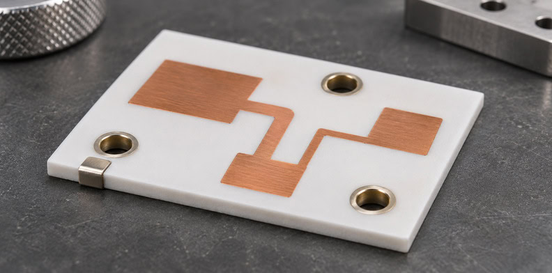
Quick Answer: Specify ceramic vias and edge connections individually: identify the metal regions that must join, those that must remain isolated, and the finished construction at each feature. Provide face views, sections and a matching net map. Ask the fabricator to confirm how its proposed ceramic construction can achieve those requirements before treating the quotation as an offer for the intended circuit.
A top pattern, a bottom pattern and a hole file can describe where features sit while leaving their electrical relationship unclear. That uncertainty affects the ceramic part the supplier must make. This guide focuses on defining ceramic vias and edge connections for a fabrication inquiry, with a worked two-sided example and a matrix you can adapt to your drawing.
Why doesn’t metallization on both sides define an electrical connection?
Metal on the front and back of a ceramic substrate describes its surface patterns. Their electrical relationship depends on whether a defined connection joins them. The drawing must show which regions join through a hole or along an edge and which remain isolated, so the supplier can evaluate the intended conductive paths.
Start by naming the metal regions. A large area on the back might be an electrically isolated heat spreader, a circuit return or another electrode. Its appearance and area alone cannot tell the fabricator which role the designer intends. Give it an identifier that can be traced between the circuit information and the physical drawing.
Consider a hypothetical two-sided substrate. The front carries a circuit with a return land, while the back carries a broad metal area. In one version, the rear metal must remain electrically isolated from that circuit. In another, it forms the return and must connect to the front land. The same general face outlines can appear in both versions; the specified interconnection changes the part.
A bare ceramic opening also needs a clear role. It may be a mechanical feature with no electrical connection, or a location where the design requires a conductor to pass between faces. Identifying a hole on a drill file establishes a location and geometry. The fabrication description still needs to say what should occupy or coat that opening in the finished substrate.
Keep the electrical names recognizable in every view. If the circuit uses a return-net name and the mechanical drawing uses region labels, provide their relationship. A note that says “connect both sides” is incomplete when either face contains several separate metal regions. The manufacturer needs to know which particular regions the connection should join.
Which finished hole constructions can a drawing request?
Distinguish an unplated opening, a hole with a metallized wall and a hole containing a specified fill. For an electrical connection, identify the conductive path and its intended contact with each face’s metal. A fill description or a drilled diameter alone does not completely define the finished interconnect.
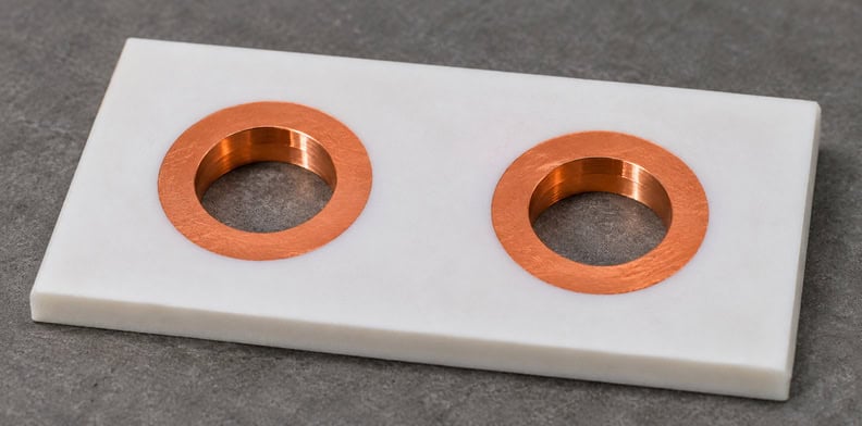
An unplated opening leaves the hole without a specified conductive wall. Its role can be mechanical, or it may accommodate a separately defined element. If the design requires electrical continuity at that location, the drawing must identify how the conductor is provided rather than asking the supplier to infer it from an otherwise mechanical hole callout.
A metallized-wall requirement describes a conductor along the hole’s interior. A wall conductor completes the intended path only where it meets the required land on each face. Show those junctions in the section so the fabricator can identify the connection at both ends of the hole.
For a filled hole, separate the fill’s function from its appearance. State whether the specified fill must conduct electricity and how it connects to the surrounding metal. The conductivity of a fill does not establish its contact with the intended land on each face; show those interfaces as well. If the proposed fill is non-conductive, any required electrical path needs a separately defined conductor. If a supplier’s proposal leaves its fill’s conductivity unspecified, ask the supplier to identify the offered construction.
The hole’s geometry can change across the ceramic thickness. LPT’s ceramic processing guidelines tell designers to identify laser entrance and exit sides and show taper in section where metallization lies nearby. That is a supplier-specific example of why a single diameter can leave geometry unclear. It does not establish a universal hole shape, process or dimensional allowance.
Show the surfaces and section locations that define your finished requirement. If the supplier’s proposed construction differs from the drawn geometry, have it mark the difference. Keep broader layout and mechanical checks with the ceramic PCB design-rules guide; this connection description supplies the detail behind its hole and interconnect check.
How is an edge connection defined differently from a hole?
An edge connection follows a specified part of the substrate boundary rather than a hole through its interior. Define the edge segment, the face regions it joins and the limits of metal coverage on each face. Relate those features to the finished outline and identify neighboring metal that must remain isolated.
A plan view may show a conductor reaching the outline without showing what happens on the sidewall. Add an edge view or a section that makes the intended path visible. Distinguish metal that stops at the face boundary from metal required to continue onto a side and meet another region.
Kyocera’s metallized ceramic substrate description includes backside circuit formation and electrode printing on side or curved surfaces. These are examples described by that supplier. They demonstrate why side-surface intent deserves a drawing view, while leaving each fabricator to confirm the particular ceramic, conductor and construction it can offer.
Give an edge feature its own identifier. If only one segment should connect a front land to rear metal, specify the limits of that segment rather than applying a whole-perimeter note. Where another conductor approaches the same edge, show the intended separation. The fabricator should be able to identify the required connection without deciding whether an adjacent metal region was meant to join it.
The relationship to singulation needs confirmation too. Singulation is the operation that separates individual substrates from an array. Ask how the proposed production sequence achieves the edge in its final state, and whether the supplier needs a different outline or local detail. The sequence depends on the supplier’s construction, so ask how the final edge is produced rather than specifying the order of operations.
A familiar laminate-PCB edge-plating note is a starting question rather than evidence of ceramic process capability. Give the ceramic supplier the finished connection intent and ask for a construction-specific response. If an edge option cannot meet it, engineering can evaluate the returned limitation before the board order assumes that connection exists.
How should a net map show connected and isolated metal?
Map each hole or edge feature to the metal regions it must join and the regions it must remain isolated from. Pair that electrical intent with a section defining the finished conductor or fill. Keep the matrix and drawing identifiers consistent so a supplier can review each requested connection without reconstructing the circuit from separate files.
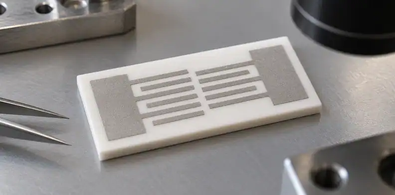
A net map describes intended electrical connections. It complements the conductor artwork by identifying which physically separate regions belong to the same electrical network. For this task, include electrically isolated metal too: a back surface used for heat spreading still needs an explicit relationship to the circuit.
Use one row per connection feature. The following blank working aid combines feature identity and drawing reference in one column. It is an editorial template, not a standard, a customer record or a description of QueenEMS’s internal process.
| Feature and geometry reference | Regions to join | Regions to keep isolated | Required finished construction | Supplier confirmation and status |
|---|---|---|---|---|
| [Hole ID; face view; section; orientation] | [Named front and back regions or nets] | [Adjacent metal excluded from the connection] | [Opening, metallized wall or specified fill; contact to lands] | [Proposed method and unresolved difference] |
| [Edge ID; segment; final-outline detail] | [Named face regions] | [Neighboring face and side metal] | [Conductive path and coverage limits] | [Proposed method and unresolved difference] |
Now complete the relevant rows for the hypothetical two-sided substrate introduced earlier. Label its front return land R and its back metal area M. These labels exist only for this example; they do not represent a supplied part or a manufacturer-approved construction.
| Hypothetical version | Connection definition | Isolation definition | Question for the fabricator |
|---|---|---|---|
| Version 1: M is an isolated heat spreader | No electrical join between R and M | Keep M isolated from the front circuit, including around holes and edges. | Does the proposed finished construction preserve that isolation? |
| Version 2: M is the circuit return | A named hole or edge feature must join R to M. | Keep that path isolated from all other named front nets. | Which section and proposed conductive construction achieve the specified join? |
Version 2, the connected-return version, needs an actual named feature, such as a specific hole with its section, rather than the general instruction “make backside ground.” Version 1, the isolated-spreader version, needs the absence of that join to remain clear. An incidental connection would change the circuit even if the front and back patterns otherwise matched the drawing.
Review a supplier’s proposed change against the relevant row. Moving a hole, extending side metal or changing a fill can affect the identified join or isolation relationship. The marked feature tells engineering which electrical intent to revisit without requiring purchasing to design the interconnect.
Why can’t one via note serve every ceramic construction route?
Ceramic constructions can realize a conductor through different material and process combinations. A generic via note may therefore leave the physical connection undefined. State the required finished geometry and electrical relationship, then ask the supplier how its proposed construction achieves them and which parts of the request it cannot confirm.
The ceramic PCB manufacturing-process comparison addresses route selection. This connection review begins with the chosen or proposed construction and asks a narrower question: what physical path joins the specified metal regions in the delivered part?
For example, a supplier’s proposal might describe a printed conductor, deposited and plated metal, or a filled interconnect within a co-fired construction. Naming one of those approaches does not by itself complete the drawing. The proposed section must still show the intended path, its contact with the face patterns and the metal excluded from that connection.
Ask the supplier to identify an unsupported request directly. A suggested alternative connection should come back as a marked construction proposal with its changed geometry and electrical relationship visible. Engineering can then consider that proposal. An unexplained “equivalent via process” leaves the buyer unable to tell whether the supplier is offering the same finished feature.
Keep a prototype proposal distinct from a production commitment. The ability to evaluate one construction on trial parts does not establish repeat production at every geometry or material combination. Ask for the scope being quoted and the remaining confirmations instead of extending one supplier example to every ceramic board.
How do continuity checks and geometry checks answer different questions?
A continuity or isolation check addresses electrical relationships between the named regions. A geometry or section check addresses the physical construction shown on the drawing. Plan the evidence for both questions where required, because an electrical result alone does not describe the hole or edge geometry, and a drawing view alone does not measure electrical continuity.

Return to the hypothetical versions. For Version 2, the connected-return version, the electrical question is whether the specified path joins R to M while remaining isolated from other nets. For Version 1, the isolated-spreader version, the intended result is different. The check must follow the released net and isolation definition rather than treating all back metal alike.
A physical inspection might address the specified hole section, location, edge coverage or contact geometry. Have the supplier identify the proposed method and what that method can establish on the actual construction. Do not assume a convenient image or measurement of a nearby feature represents an inaccessible interface.
Keep the connection matrix revision, feature sections and confirmed construction with the quotation and release drawing. If a confirmation remains open, name the affected feature and question. That gives purchasing a concrete item to resolve before ordering, while the supplier and design owner retain responsibility for the proposed method and applicable acceptance requirements.
Frequently Asked Questions
If both sides of a ceramic substrate are metallized, are they connected?
Only where a defined conductive path joins them. Identify the particular metal regions and the hole or edge feature that connects them. Metal areas can be present on both faces while the design requires electrical isolation between those areas.
Does drilling or laser-cutting a hole define its metallization?
No. Creating an opening establishes a physical feature. A conductive wall or other interconnect needs its own finished-construction requirement and supplier confirmation. Show the intended contact with each face’s circuit metal as well as the opening geometry.
Does a filled hole prove a front-to-back connection?
No. Identify whether the specified fill is conductive and how the required path contacts both face patterns. A material description, appearance or filled opening alone does not establish the intended electrical connection in the completed substrate.
Can the same via note be used for every ceramic process?
Define the finished connection intent consistently, but obtain a response for the proposed construction. The supplier must explain how that construction achieves the required join and isolation. A note accepted for one ceramic route does not confirm another route’s capability.
Send your released files for a quote and free DFM review.
Send ceramic drawings with via and edge-metallization details for review. Define isolated areas, net connections and inspection requirements.
If parts will be fitted to the ceramic substrate, add their BOM and placement details. Identify customer-supplied items and confirm supported attachment methods.