
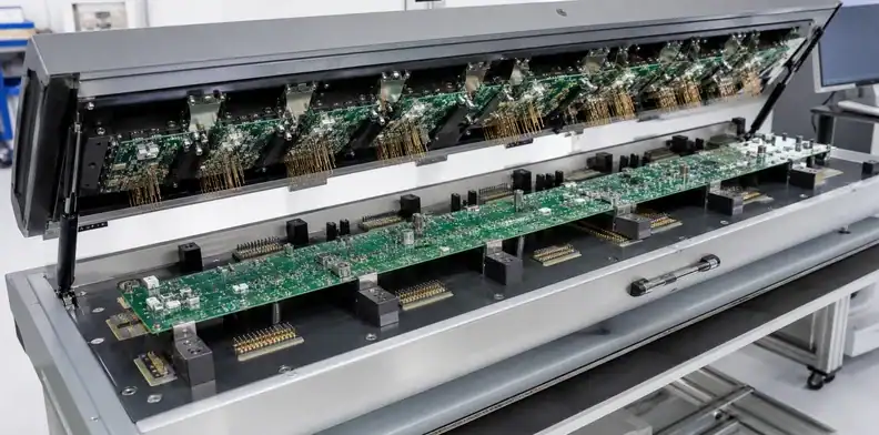
Quick Answer: A large PCB test fixture must balance probe and hold-down forces locally so the unit under test does not become the fixture’s spring. Map total probe force by zone, place counter-support near concentrated loads, locate from functional datums and verify board deflection during contact. Electrical coverage can be correct while poor mechanical support creates false opens or damages solder joints.
Hundreds of spring probes engaging together can apply a substantial combined load. A small assembly may tolerate an imperfect support pattern; a long board can bend between sparse posts, change probe stroke and strain components near dense test-point clusters. Large PCB test fixture design therefore begins with the force map and board geometry, not with a list of nets alone.
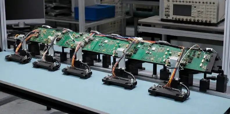
An ICT or FCT fixture must support the assembly and locate it consistently under probe and clamping loads. Agree on electrical-test coverage before specifying the tooling, and document fixture ownership and storage responsibilities separately from its mechanical design.
Table of Contents
- Define the test method and mechanical risk
- Map total probe force by board region
- Place counter-support near concentrated loads
- Locate the board without forcing its shape
- Separate false failures from real defects
- Protect powered tests and signal integrity
- Qualify and maintain the fixture
- Send a fixture-ready RFQ package
- Lock fixture configuration ownership
Define the test method and mechanical risk
The fixture concept must follow the electrical test method, access side, component state and production volume. A bed-of-nails ICT with dense bottom probes creates a different force system from a functional fixture that contacts several connectors and supports the board horizontally.
Bare board and assembled board need different protection
A bare board may be tested with electrical contact across exposed pads and can use laminate support areas that later contain components. An assembled board introduces fragile ceramic parts, BGAs, bottom-side devices and tall hardware. The support drawing needs the actual populated STEP model, not only the fabrication outline.
Define whether the board enters free, in a product frame or on a process carrier. The fixture should not silently flatten a warped input because that may hide the incoming condition and load joints during test.
Choose contact architecture before test-point release
ICT, flying probe, connectorized functional test and hybrid methods have different access, force, speed and evidence. The PCB design-for-test review can establish accessible targets and test intent before the mechanical tool is committed.
If large-board geometry makes a full bed-of-nails fixture impractical, changing the method may be safer than concentrating probes into unsupported zones. Record the coverage tradeoff instead of assuming every schematic node requires a spring probe.
Evidence check: Do not release test points until the board condition, contact method, access side and support concept are reviewed together.
Map total probe force by board region
Probe force should be calculated at working stroke and summed by zone, not estimated from probe count alone. Different probe series, tip geometries and stroke settings can produce different loads, while fixture tolerance and board flex can change actual compression.
Build a coordinate-based force table
Export test-point coordinates, probe type, nominal working force and access side. Group the points around BGAs, connectors, power stages and other dense areas. A fixture with acceptable total force can still bend the board locally when many probes sit inside a small region.
QA Technology explains that spring-force choice affects contact reliability, cycle life and possible UUT damage. Use the selected manufacturer’s working-stroke data rather than a generic force per probe. For an illustrative zone with 80 probes at 0.9 N and 40 probes at 0.5 N, the upward probe total is 80 x 0.9 + 40 x 0.5 = 92 N. This assumed total is not an allowable PCB load: plot its coordinates, counter-support and clamp reactions, then validate local deflection or strain at the actual working stroke.
Check the actuation system and reaction path
Vacuum, pneumatic, mechanical and manual fixtures deliver force differently. Confirm that the frame and pressure plate remain parallel and that the actuation margin covers all probes without forcing excessive overtravel. Include top-side pushers and bottom stoppers in the force balance.
The force map should show upward probes, downward pressure fingers, support posts, clamp reactions and fragile component keep-outs on one coordinate system.
Force rule: Approve the fixture from the worst local unbalanced load and working stroke, not only the sum of probe catalog forces.
Place counter-support near concentrated loads
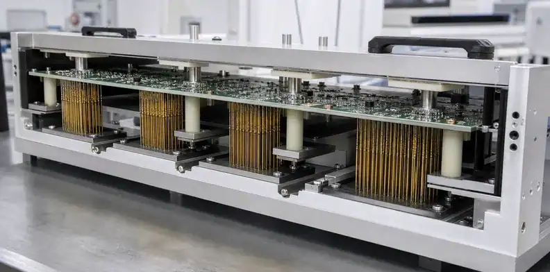
Counter-support should oppose probe force as locally as component clearance allows. A support post at the board perimeter cannot fully react a dense probe cluster in the center of a large unsupported bay.
Map safe reaction points around the load
| Fixture zone | Preferred support action | Conflict to resolve | Evidence |
|---|---|---|---|
| Dense BGA test field | Counter-support around the package footprint | Bottom components and solder joints | Force/deflection map |
| Connector pin field | Support near connector body/mounts | Mating access and housing clearance | Contact sequence trial |
| Thin open laminate | Distributed posts or plate support | Trace/via and coating contact | Approved support map |
| Edge test pads | Stable edge rail plus local reaction | Gold fingers or bevel protection | Contact-zone drawing |
| Mixed top/bottom probes | Opposed stops and pressure fingers | Component height variation | Loaded fixture section |
Support posts need flat, robust contact areas that do not sit on components, solder joints, exposed test pads or prohibited copper. Their diameter, height tolerance and material should be controlled. A very small hard post may reduce global sag while creating local stress.
Resolve clearance and variant conflicts
When component density prevents ideal counter-support, evaluate lower-force probes, redistributed test access, a pressure plate with safe contact points or a different test method. Finite-element analysis can help on critical assemblies, but the model still requires actual loads, restraints and material assumptions.
Do not assume that more support posts always improve the tool. Extra posts can land on solder mask over vias, collide with alternate BOM variants or establish a different plane from the primary supports. Classify supports as load-bearing, anti-sag or setup-only, and give each one a height tolerance tied to the same fixture datum.
For variants built on the same PCB, overlay the maximum component envelope from every fitted option. A stopper safe for the base model may contact a component used only on the high-feature version. The fixture drawing and test program should identify which support configuration belongs to each assembly variant.
Locate the board without forcing its shape
The fixture should locate the PCB repeatably from functional tooling features while allowing outline and hole-position tolerance. Tooling pins are for position; support posts are for force. Combining both functions at every contact can over-constrain a long board.
Establish primary, secondary and clearance features
Use one primary datum feature, a secondary feature that controls rotation and clearance at other locators. Match the fixture coordinate system to the released fabrication and assembly data. The PCB datum-control method helps prevent fixture coordinates from drifting away from product-critical relationships.
Pins require lead-in, correct finished-hole assumptions and clearance for loading. Do not force a pin into a plated functional hole without engineering approval.
Record which locator establishes each axis so maintenance cannot reverse the intended datum hierarchy.
Sequence clamps and probes predictably
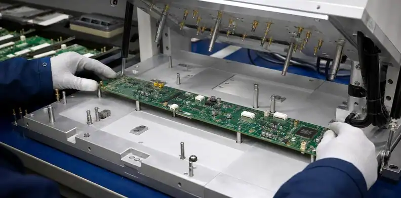
Seat the board on its intended supports before probes reach working stroke. Clamp or vacuum sequence should not drag the board across locator pins or push one corner down while the opposite corner remains free. Observe the first article at slow actuation and measure whether the board lifts from any support.
Location check: The UUT must reach its datum and support state before electrical contact force is applied.
Separate false failures from real defects
Contact problems caused by board flex can appear as intermittent opens, unstable resistance or failures that disappear when an operator presses the fixture. The reaction plan should test mechanical contact quality before sending a good assembly to rework.
| Symptom | Possible fixture cause | Diagnostic check |
|---|---|---|
| Failure changes between cycles | Variable board seating or probe stroke | Measure seating and repeat without moving cables |
| Clustered opens near one BGA | Local board deflection | Compare support and force map in that zone |
| Passes when lid is pressed | Insufficient/uneven actuation | Measure pressure-plate parallelism and working stroke |
| Pad damage or witness marks | Excess force or wrong tip | Inspect target, probe and stroke setting |
| Failure after fixture maintenance | Stopper/pusher height changed | Verify tooling revision and setup record |
Use a known-good correlation board and a controlled failing sample when possible. Repeat several cycles without removing the UUT, then repeat after unloading and reloading. The first set tests contact stability; the second adds location and operator variation.
For complex large-board evidence, send the test-point and component-height maps through a QueenEMS test/DFM assessment. The review can flag support conflicts and data gaps before fixture machining; it does not replace product-level test coverage approval.
Failure call: Do not authorize component rework until contact stability, seating and local support have been checked against the failing coordinates.
Protect powered tests and signal integrity
Functional testing adds power, high current, communication channels, connector mating and operator safety. Mechanical support remains necessary, but fixture wiring and grounding can create failures that resemble board defects.
Keep high-current paths short and sized for the load; provide a defined return path; separate sensitive measurement connections from switching noise; and document cable/connector identity. Long fixture cables can add delay, loss or pickup that is absent in the product. For controlled interfaces, compare the fixture path with the board’s controlled-impedance design requirements.
Connectorized functional tests should control mating depth, insertion direction and cycle count. The fixture must react connector force through the frame rather than through a long PCB span. Use keyed interfaces and strain relief so an operator cannot transfer cable load into the unit while diagnosing a result.
Guard energized contacts and use interlocks appropriate to the voltage, stored energy and actuation. Define emergency stop, discharge time and safe access in the fixture requirement. These are product/test-engineering responsibilities, not assumptions left to the PCB fabricator.
Mechanical strain measurement may be appropriate near large BGAs, ceramic components or press-fit connectors during fixture qualification. Place gauges and set limits under the customer’s reliability method; there is no one strain limit that applies to every assembly and package.
Powered-test boundary: Electrical pass/fail data is valid only when the fixture path, safety state and mechanical contact condition are within the qualified setup.
Qualify and maintain the fixture
Qualification should prove repeatability, coverage, mechanical stability and safe operation on the actual board revision. Record probe plate, support plate, pushers, software, wiring and test-program revisions as one controlled tool configuration.
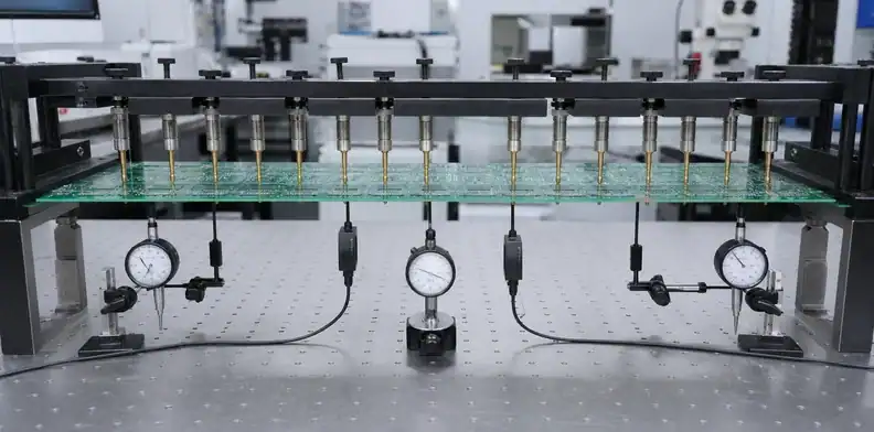
Run repeated cycles with correlation boards and inspect high-force regions for witness marks, pad damage or changing deflection. Challenge loading variation within normal operator and board tolerances. Verify that supports remain in contact and that the pressure plate does not dome under load.
Measure a small set of mechanical setup characteristics before electrical correlation: board seating at reference supports, pressure-plate travel, vacuum or actuator state, and contact witness at selected probes. These measurements make later troubleshooting faster because the accepted electrical result is tied to a known mechanical configuration.
After fixture repair, requalify the affected zones rather than assuming that a replaced plate or guide pin restores the old geometry. A new machined part can be within its own drawing tolerance and still shift the combined support/probe relationship.
Maintenance criteria should address probe cleaning/replacement, stopper and pusher height, vacuum seals, guide pins, cables, connectors and fixture flatness. A probe replacement with different spring force or travel is a configuration change, not an interchangeable consumable choice.
Keep a failure log by coordinate and symptom. Rising retest rate in one zone may reveal contamination, worn probes, loose support or alignment drift before the fixture produces widespread false failures.
Send a fixture-ready RFQ package
Provide the fixture designer and assembler with one reconciled data package.
| RFQ input group | Minimum content |
|---|---|
| Product data | Gerber/ODB++, drill, fabrication/assembly drawings, BOM and centroid/CPL variants |
| Mechanical model | Board STEP model, top/bottom component heights, datums, tooling holes and prohibited contact zones |
| Electrical access | Test-point coordinates, access side and function |
| Probe assumptions | Probe family, tip, working force and stroke |
| Production and evidence | Volume, cycle expectation, changeover, safety, reports and correlation-board requirements |
Send the package through the QueenEMS large PCB manufacturing review so fabrication, assembly, board support and test access can be compared before quotation. For a fixture-specific request, submit the force map and test data to QueenEMS and ask for a quote that identifies fixture ownership, first-article evidence and excluded test development.
Lock fixture configuration ownership
A fixture is a controlled production system, not only machined hardware. Assign ownership for the mechanical plates, wiring, probe list, test program, correlation board and maintenance record. Define who approves changes and which evidence is required after repair. This prevents a mechanically altered fixture from continuing under an old electrical qualification record.
Record rule: Machining and later revisions should proceed only when PCB revision, test program, probe map, support map and commercial ownership are aligned in one configuration record.
FAQ
Can probe force damage a large PCB assembly?
Yes. Unbalanced local force can flex the board, damage pads or strain components and solder joints. Calculate working-stroke force by region and place counter-support near dense probe areas.
Should support posts sit directly under BGAs?
Only on approved board areas with component and solder-joint clearance. Often the practical solution is support around the package footprint or a pressure feature on a safe top-side zone rather than contact beneath joints.
Does vacuum actuation prevent board flex?
No. Vacuum provides actuation force, but the UUT can still bend between support points or under dense probe clusters. Validate the loaded mechanical shape.
How can I identify a fixture-related false failure?
Repeat the test without unloading, compare after reload, inspect seating and correlate failing coordinates with the force/support map. A result that changes with lid pressure or support adjustment needs fixture investigation.
Who owns the fixture design?
Define ownership in the purchase package. The customer normally owns product test intent and acceptance; the fixture/test provider owns the implemented tool within agreed inputs; the assembler operates and maintains the released configuration.
Sources
Written by the QueenEMS Engineering Team
Upload your files today · Free DFM check before production · Ship worldwide
Get your PCB prototypes in as fast as 24 hours. We handle FR4, Rogers, and hybrid boards up to 40 layers in volume production, with advanced builds subject to engineering review — free prototypes for 2–4 layer FR-4 boards, no minimum order.
Just upload your Gerber + BOM — we source every part, assemble, and inspect (AOI + X‑Ray) so you don't have to chase suppliers. Boards ship in as fast as 24 hours.