
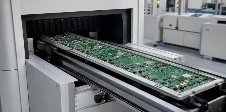
Quick Answer: A large PCB reflow carrier is needed when the bare assembly cannot travel, remain supported or protect underside features through printing, placement and reflow. Design the carrier around the loaded equipment envelope, neutral support zones, component clearances and thermal transparency. Qualify the board and carrier together with the actual oven orientation and thermocouple locations.
A carrier can keep a long board on the conveyor and still create a poor soldering process if it adds excessive thermal mass, shadows one region or clamps the laminate at the wrong points. Large PCB reflow carrier design must solve both mechanics and heat flow. Treating the tool as a simple flat tray leaves the most consequential decisions undocumented.
Check equipment-size compatibility across the assembly route before designing a carrier. Once the board needs dedicated support, qualify the carrier geometry, the loaded thermal profile and the conditions for maintaining and reusing the tool.
Table of Contents
- Decide whether a carrier is necessary
- Fit the loaded carrier through the full route
- Design support, location and component clearance
- Reduce thermal mass and heat shadow
- Build a representative reflow profile
- Verify board shape and soldering results
- Control carrier revision, cleaning and wear
- Quote a carrier-ready assembly
Decide whether a carrier is necessary
Use a carrier when the PCB cannot be conveyed, supported, located or protected repeatably in its own released outline. Large size alone is not enough: a thick rectangular board with clear conveyor edges may run without tooling, while a thinner, routed or bottom-populated board may need support at a smaller outline.
Establish the no-carrier baseline
First confirm how the board behaves on the exact printer, placement machine and oven rails. Review thickness, edge support, orientation, mass distribution, cutouts and temperature-related sag. A center support available in one oven does not prove another line has the same configuration.
Record the observed or predicted failure: rail instability, excessive span, edge components, underside collision, fiducial access, placement support or reflow deformation. This keeps the carrier design targeted.
Define carrier triggers
Typical triggers include irregular outlines that cannot ride parallel rails, thin boards that sag between rails, large cutouts, heavy components, bottom-side parts near conveyor edges, flex/rigid-flex regions and a need for one datum through several SMT operations.
A carrier is not a substitute for fixing a fundamentally unbalanced PCB construction. Use large PCB warpage controls for stack-up, copper and fabrication causes; use the carrier for process support that remains after those controls.
Decision point: Create tooling only after the unsupported failure mode and the operations that need the tool are named.
Fit the loaded carrier through the full route
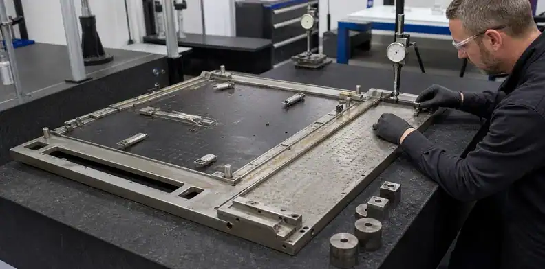
The true processed object is the loaded carrier: carrier length, width, thickness, mass, top/bottom clearance and datum—not the PCB alone. Every machine and transfer must accept that combined envelope.
Check rails, center supports and transfers
Document rail-contact width, conveyor range, center-support availability, board-height reference and transfer gaps. A carrier lip that works in the printer can catch at an inline conveyor or change the board height expected by placement.
Measure the maximum unsupported transfer gap with the loaded carrier, not with an empty fixture.
KIC’s profiler-carrier information distinguishes configurations for ovens with and without center support. This is a carrier for profiling equipment; its compatibility does not qualify a production PCB support pallet or prove the assembled product’s thermal profile. Record the production carrier’s own clearance and loaded support condition separately.
Confirm clearance in every direction
Include clamps, handles, locators and any top cover in the envelope. Check printer stencil clearance, placement nozzle/camera access, reflow tunnel height, AOI grip and unload method. The carrier should not require an operator to touch or rotate a freshly printed board between machines.
The carrier drawing needs a travel arrow and board side. Treat rotation or flipping as a controlled setup, not an informal workaround.
Envelope rule: Equipment approval must reference the loaded carrier revision and travel orientation, not only the finished PCB dimensions.
Design support, location and component clearance
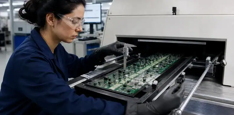
Support should react gravity, conveyor motion and process forces through neutral laminate areas while keeping solder paste, components, joints and inspection targets clear. The carrier must locate the board repeatably without forcing it into a shape.
| Tool feature | Purpose | Main conflict | Required input |
|---|---|---|---|
| Edge step/rail | Conveyor transport | Edge components and bevels | Board edge map |
| Support lands | Reduce sag | Bottom pads, vias, components | Bottom STEP model |
| Tooling pins | Position board | Hole tolerance and functional holes | Datum drawing |
| Retainers/clamps | Prevent lift or shift | Top components and thermal restraint | Component envelope |
| Pockets | Clear underside parts | Reduced tool stiffness and heat flow | Height and keep-out map |
| Carrier fiducials | Machine registration | Camera contrast and stencil access | Equipment vision needs |
Use primary and secondary locating features plus clearance at additional points. A long board should not be pressed over several tight pins. Retainers must hold against lift and travel without turning thermal expansion into in-plane strain.
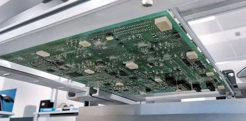
Bottom pockets require enough clearance for component tolerance, solder joints and loading variation. Thin walls around deep pockets may reduce carrier stiffness, so inspect the tool structure as well as the PCB.
Loading and unloading features deserve equal attention. Provide finger relief or handles outside the heated product area, a positive indication that the PCB is fully seated, and retainers that cannot be left half engaged. A carrier that requires an operator to press on the board center during loading defeats the support design before it reaches the oven.
Where carriers enter automatic equipment, verify sensor targets and optical contrast. Dark composite material, reflective inserts or deep pockets can change board-presence and fiducial detection. Machine recognition should be tested under production lighting and after normal carrier wear.
Reduce thermal mass and heat shadow
Carrier geometry and material change how the assembly heats and cools. Remove unnecessary material while preserving stiffness, keep supports away from solder joints where possible and profile the exact loaded tool instead of applying a board-only recipe.
Balance stiffness and thermal transparency
A thick plate may support the PCB well but delay heating near broad contact areas. Large cutouts reduce mass but can let the carrier warp or sag. Use ribs, pockets and local lands purposefully rather than selecting one uniform thickness by habit.
High-temperature, dimensionally stable, ESD-appropriate carrier materials are commonly used, but material name alone does not prove performance. Request data for the intended temperature cycles, machining geometry, cleaning chemistry and service environment.
Avoid local heat shielding
Clamps, bars and pockets can change convection and radiation around components. Compare high-mass parts, shielded areas and carrier-contact zones in the profile plan. A carrier that creates a colder region may tempt engineers to raise the entire oven recipe and overheat a different region.
The reflow profile optimization method provides process background; the carrier qualification must add tool-specific thermocouple locations.
Evidence check: Minimize carrier material around the product where mechanics allow, then prove the loaded thermal result rather than assuming transparency.
Build a representative reflow profile
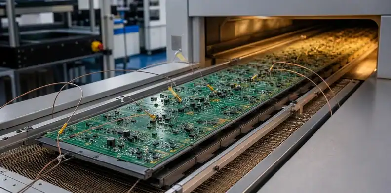
Attach thermocouples to locations that represent likely cold, hot, high-mass and carrier-influenced regions. The oven set points are not the product profile; the measured solder-joint or package environment is what must meet the approved process window.
| Thermocouple location | Why it belongs in the profile |
|---|---|
| Large central component or copper mass | Likely slow-heating region |
| Small exposed component away from carrier | Potential fast/hot region |
| Board area adjacent to a support land | Detects carrier heat shadow |
| Far end of the long travel axis | Reveals spatial oven/product difference |
| Connector or heat sink region | Represents local mass and airflow change |
| Sensitive component identified by supplier | Checks component-specific limit |
Use secure attachment appropriate to the measured point and document exact coordinates. Profile with normal carrier loading, board orientation, conveyor speed and production spacing. An empty carrier or a thermocouple floating in oven air does not reproduce the assembly.
Record the attachment material, bead position, channel name and wire routing that could lift a sensor from the joint. A repeat profile is comparable only when the measurement setup is controlled as tightly as the oven recipe.
If the carrier is used for both sides, profile the relevant first- and second-side configurations. Existing bottom-side components and pockets change mass and airflow. The contextual review package should include the thermocouple map, and the QueenEMS assembly DFM path can identify missing geometry or component constraints before the first trial.
Record rule: Tie the accepted recipe to the board, carrier and component-population revision used during measurement.
Verify board shape and soldering results
Carrier qualification is complete only when the board remains mechanically acceptable and the soldering evidence meets the assembly plan. A flat-looking tool does not prove the PCB stayed supported through peak temperature and cool-down.
Measure board condition before loading, after carrier seating, after reflow while using the agreed cooling state and after unloading. Use the same support/datum method for comparisons. Inspect whether clamps left marks, whether the board lifted from support lands and whether any component touched a pocket or retainer.
Cooling deserves its own observation. A board may remain constrained while hot and change shape as the carrier and laminate cool at different rates. Define the unload temperature or waiting condition used for measurement, and do not compare one board immediately after the oven with another after a long bench cool.
Where the carrier continues into AOI or test, confirm that the accepted reflow support does not hide inspection fields or alter test support. If the board is removed, document the unloading sequence and support provided during that transition.
Review paste/reflow outcomes near carrier contact, large copper areas and both ends of the board. Use SPI/AOI/X-ray or joint inspection appropriate to the assembly risk; the carrier does not define the product acceptance method.
| Result | Likely next action |
|---|---|
| Board sags inside carrier | Add/reposition support or revise carrier stiffness |
| Cold joints near support mass | Reduce heat shadow or reprofile the loaded tool |
| Edge lift at peak/cooling | Review retainers, board construction and restraint |
| Component/pocket contact | Correct clearance and tolerance stack |
| Good board but warped carrier | Change tool structure/material and reject worn tools |
Acceptance boundary: Approve both the product result and the carrier condition; one cannot substitute for the other.
Control carrier revision, cleaning and wear
A production carrier is a controlled tool. Give it a unique part number, revision, compatible PCB revisions, orientation mark and inspection record. Include the released geometry, support/contact map and material with the tooling record. After changes to pocket geometry, support contact, clamps or thermal mass, assess and measure the affected product profile before reusing its previous release. The Binghamton oven-versus-board profiling study distinguishes process characterization from subsequent oven verification; its studied board and conditions do not make oven verification a substitute for qualifying a changed product-carrier combination.
Define incoming inspection for flatness, damaged pockets, worn locators, loose clamps, contamination and identification. Cleaning chemistry and method must suit the carrier material and residues without swelling, eroding or distorting the tool.
Track cycle count only when it relates to a validated inspection or replacement method; do not publish a universal lifetime. High-temperature cycling, mishandling and aggressive cleaning can age tools differently. A carrier that no longer seats flat should be quarantined even if it has not reached an administrative cycle target.
Store carriers on supports that preserve their own flatness. Leaning a wide tool against a wall or stacking it on protruding clamps can create deformation that later appears as a board problem. The storage rack should contact stable tool zones, identify orientation and protect locators from impact.
Cleaning verification should inspect pockets, vacuum holes, clamps and fiducial surfaces for flux or paste residue. Record prohibited solvents and maximum cleaning temperature from the tool material data. A clean-looking top surface does not prove that a locator can return freely or that a pocket remains at the released depth.
When board data changes, compare component envelopes, fiducials, tooling holes, paste regions and mass map before declaring the tool compatible. Record modifications on the drawing and tool itself.
Quote a carrier-ready assembly
Prepare a package that lets tooling and assembly engineers model the loaded route:
- PCB Gerber/ODB++, drill, paste layers and fabrication drawing
- Board and enclosure/fixture STEP models
- BOM and centroid/CPL with fitted variants
- Top and bottom component height/keep-out maps
- Tooling holes, fiducials, conveyor edges and travel orientation
- Printer, placement, oven and inspection envelope constraints
- Required thermocouple locations and component limits
- First-article quantity, evidence and tool-ownership terms
Send these inputs through the QueenEMS large format PCB assembly review. QueenEMS can compare carrier needs with fabrication and line constraints and return quotation assumptions, tooling scope and first-article questions. For a project review, submit the carrier and assembly data to QueenEMS and ask that tool revision, profiling scope and ownership be itemized.
Quotation boundary: Do not release the carrier until its machine envelope, support map, thermal-profile plan and board revision agree.
FAQ
Does every large PCB need a reflow carrier?
No. A self-supporting board with suitable conveyor edges and verified flatness may run without one. Use a carrier when transport, sag, underside clearance or common datum control cannot be achieved repeatably.
Can the carrier make reflow problems worse?
Yes. Excess thermal mass or shielding can create cold regions, while rigid restraint can stress the board. Profile the actual loaded carrier and inspect product shape and joints.
Should clamps hold the PCB tightly during reflow?
They should prevent unsafe movement without forcing the board flat or blocking thermal expansion. Define contact zones, clearance and restraint direction in the tool drawing.
Can one universal carrier serve several boards?
Sometimes in high-mix production, but each board still needs verified support, location, clearance and profile. A universal frame does not make the inserts or setup universal.
What files are needed to quote the carrier?
Provide PCB data, STEP model, BOM/CPL, component-height map, machine constraints, travel orientation, profile requirements and first-article evidence expectations.
Sources
- KIC carrier solutions for large-PCB thermal profiling
- Binghamton University oven and board profiling study
Written by the QueenEMS Engineering Team
Upload your files today · Free DFM check before production · Ship worldwide
Get your PCB prototypes in as fast as 24 hours. We handle FR4, Rogers, and hybrid boards up to 40 layers in volume production, with advanced builds subject to engineering review — free prototypes for 2–4 layer FR-4 boards, no minimum order.
Just upload your Gerber + BOM — we source every part, assemble, and inspect (AOI + X‑Ray) so you don't have to chase suppliers. Boards ship in as fast as 24 hours.