
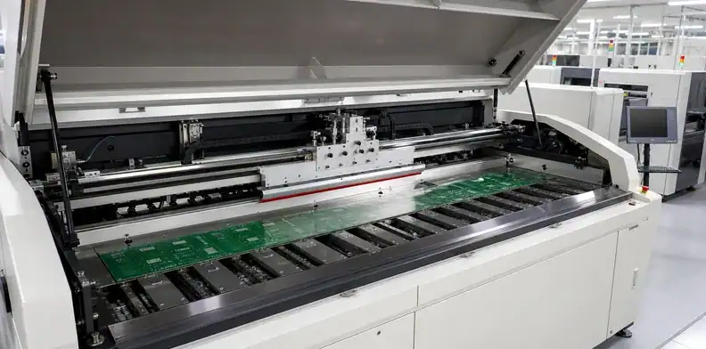
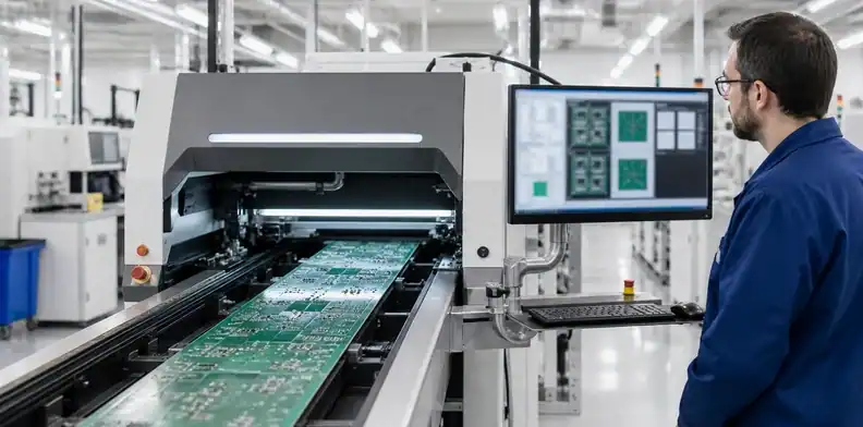
Quick Answer: Oversized PCB solder paste printing is qualified by four physical windows: board size, usable print area, stencil frame and board-support range. A printer that can transport the outline may still lack full squeegee travel, stencil clearance or support under every aperture. Printing in two passes is a controlled exception for separated regions, not a general workaround for an undersized printer.
Solder paste printing establishes the deposit volume and position that placement and reflow must use. On a long board, small alignment, support or stencil-release errors can change across the span. The correct question is not simply whether the board fits inside a machine; it is whether the released paste pattern can be printed, separated and inspected in one repeatable route.
The broad large format PCB assembly equipment review identifies printing as one line constraint. This article goes deeper into the printer, stencil, support and evidence required for oversized PCB solder paste printing.
Table of Contents
- Qualify all four printing windows
- Build full-area support and gasketing
- Design the stencil for the component mix
- Control alignment and stencil release
- Decide whether two-pass printing is acceptable
- Inspect deposits across the complete board
- Run a controlled printing first article
- Quote the actual printing route
Qualify all four printing windows
The usable printing limit is the smallest compatible window among the PCB transport range, printable area, accepted stencil frame and support-table geometry. Equipment brochures often list these values separately because they describe different mechanisms.
Rated PCB size is not the printable area
A conveyor may transport a board beyond the area that the squeegee can cover or the vision system can align. Yamaha’s YSP20, for example, publishes an applicable PCB range and specific stencil formats; FRITSCH publishes PCB, stencil and printing-area values for its oversized model. Those numbers illustrate why qualification must use the exact machine model and configuration rather than a generic “large printer” label.
Record length, width, thickness, travel orientation and edge-clearance needs. Add the actual paste bounding box—the smallest rectangle containing every aperture. A board may be long because of a mechanical tail while its printed region remains within a smaller window, or the opposite may be true.
Orientation changes more than footprint
Rotating the board can place the long axis within printer travel, but it also changes conveyor support, squeegee stroke, stencil foil behavior and downstream orientation. Confirm that the same rotation works at solder paste inspection (SPI), placement and transfer. Avoid a route that requires an operator to rotate a printed board by hand while paste is exposed.
Qualification rule: Approve the printer only when the released paste bounding box, stencil frame and support map fit the exact configured machine.
Build full-area support and gasketing
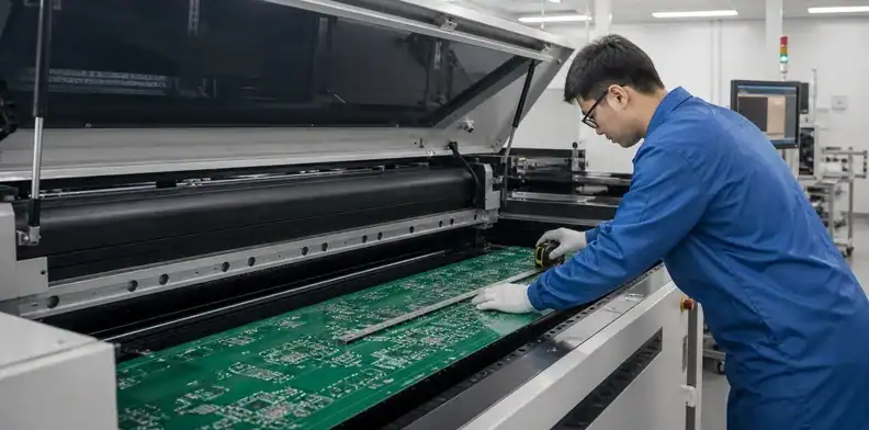
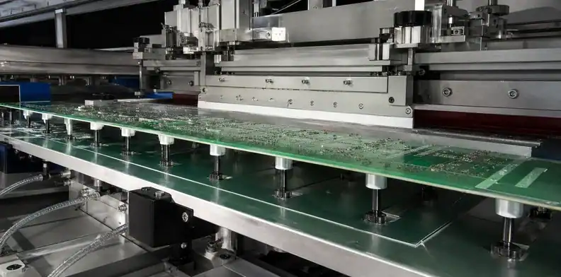
Every printed region needs support that keeps the PCB in intimate, repeatable contact with the stencil. Unsupported areas deflect under squeegee pressure, weaken gasketing and can produce smearing, insufficient deposits or variable release.
Map support beneath the paste apertures
Start with a bottom-side STEP model and paste Gerber. Place support where it reacts printing force without touching components, protruding leads, vias requiring clearance or fragile features. For a bare first side, vacuum support or a dedicated tooling plate may be possible. For the second side, pockets and selective supports must clear existing components.
The support map should include pin/plate coordinates, height, material and which board revision it serves. “Use standard pins” is not enough for a board with wide unsupported bays.
Preserve a continuous stencil seal
Board bow, uneven support or edge features can open a local gap between stencil and pad. That gap lets paste spread beneath the foil instead of filling only the aperture. Check the board in its actual supported condition before tuning squeegee pressure to compensate.
A dedicated carrier can standardize support through printing and placement, but the loaded carrier becomes the processed object. Confirm fiducials, clamping, top-surface height and stencil clearance with the carrier installed.
The large PCB fiducial requirements help define stable global and local references, while the support drawing controls the physical seal.
Print boundary: Do not correct board movement or poor gasketing by increasing squeegee pressure until the support condition is verified.
Design the stencil for the component mix
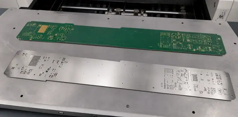
Stencil thickness and aperture geometry must deliver compatible paste volumes for the smallest and largest joints across the board. Oversized foil does not change the area-ratio physics of each aperture, but the long span adds foil support, frame rigidity and release considerations.
| Design input | What it controls | Large-board concern |
|---|---|---|
| Paste-layer Gerber | Aperture location and shape | Full pattern must fit the usable print area |
| Component/package list | Required deposit volumes | Fine pitch and large thermal pads may conflict |
| Stencil thickness | Deposit height and release | One thickness serves distant component regions |
| Step-up/step-down areas | Local volume adjustment | Step transitions need clearance and supplier review |
| Frame and foil size | Tension and machine fit | Large foil must remain stable through the stroke |
| Cleaning access | Aperture recovery | Long stencil needs complete underside-cleaning coverage |
Infineon package guidance illustrates how stencil thickness, aperture reduction and SPI measurement depend on package geometry. Apply component-specific recommendations to the actual BOM instead of assigning one reduction percentage to the entire board.
For exposed pads, fine-pitch devices and large connectors, show the assembler the released land pattern and paste intent. Engineering should approve volume changes; the stencil supplier or assembler may propose manufacturable aperture adjustments but should not silently redefine the design.
Control alignment and stencil release
Alignment must remain accurate from one end of the print field to the other, and stencil separation must release deposits without dragging them. A long board can expose scale, rotation or local distortion that a single central reference does not reveal.
Use references that reveal span error
Place global fiducials so the printer can observe translation and rotation across the working area. Local fiducials may be needed near fine-pitch devices when board and stencil behavior across the span cannot be represented by one global correction. Confirm that carrier apertures, clamps and stencil hardware do not hide the marks.
Vision correction cannot fix a support-induced change during the squeegee stroke. Compare first-article offsets near both ends and the center to distinguish a global alignment error from local board or stencil behavior.
Qualify separation over the long path
Controlled separation lets paste release from apertures while the board remains seated. On a large stencil, release timing and foil movement may vary across the area. Inspect deposit shape, not only machine alarms. Smearing, dog-ears or directional tails can indicate local gasketing or release problems.
Include stencil underside cleaning in the program and confirm the mechanism covers the complete used area. A nominal cleaning cycle that misses the far end of an oversized frame does not restore the process.
Alignment check: Approve the print only after deposit position and shape are compared at both ends, the center and the most demanding package regions.
Decide whether two-pass printing is acceptable
Two-pass printing should be considered only when the paste regions are physically separated, each pass has independent reliable registration and the second setup cannot disturb deposits from the first. It is not a safe default for a continuous aperture field or a shared fine-pitch region.
| Situation | Decision | Reason |
|---|---|---|
| Two isolated component zones with a clear no-paste gap | Consider after first-article proof | Pass boundary can be kept away from deposits |
| Continuous pad field crossing the proposed split | Reject | Registration and paste disturbance affect functional joints |
| Second pass requires contact over printed deposits | Reject | Stencil, fixture or handling can smear the first print |
| Separate stencils use different datums | Reject until a common datum strategy exists | Offset cannot be reconciled reliably |
| Low-volume hand process without complete SPI | Use only under explicit engineering deviation | Evidence and repeatability are limited |
The second pass changes work time, paste exposure, board movement, cleaning and inspection sequence. Define which pass occurs first, how the board remains supported, where the stencil edge travels and how a misprint is cleaned without contaminating the other region.
Before accepting the exception, ask whether a larger printer, redesigned panel, detachable tail, separate module or different assembly partition gives a cleaner production route. The one-large-PCB versus multiple-board comparison can support that system-level decision.
For an early feasibility check, send the paste layers, outline and proposed split region through the QueenEMS SMT/DFM review. The desired return is a route question list—not a promise that every split print is producible.
Exception boundary: Do not release two-pass printing until the overlap-free regions, common datum, support state and full-board inspection plan are written.
Inspect deposits across the complete board
SPI should measure the printed regions that matter, using a recipe and field capable of the board’s complete paste pattern. A pass result from one subsection cannot prove the opposite end of an oversized PCB.
Build a first-article coverage map
Measure volume, height, area and positional offset where the available SPI supports them. Select representative locations near both ends, the center, fine-pitch devices, large thermal pads and any region with unusual support. Record board orientation and carrier state with the results.
If the board exceeds automatic SPI range, map every uncovered pad and define how its required deposit characteristics will be verified. Visual checks cannot measure volume; whole-board weighing and a process coupon do not establish pad-by-pad volume, height, area or offset on the product. For a hypothetical two-pad example, 0.12 + 0.04 mm3 and 0.08 + 0.08 mm3 both total 0.16 mm3, despite different distribution; these values are not acceptance limits. Use a qualified measurement route that covers the required characteristics, or document the remaining coverage gap for engineering disposition before release. Infineon’s board-assembly recommendations, section 3.1, explain paste-volume risks and recommend SPI for the covered small leadless packages; qualify the method for the actual package and board.
Link defects to a reaction plan
A deposit failure should trigger a named action: stop printing, quarantine boards since the last accepted check, inspect/clean the stencil, verify support and paste condition, then reprint a controlled sample. Do not let placement continue while the team debates whether an end-of-board offset is acceptable.
The solder paste inspection record should identify the measurement fields and limits used for release when SPI is part of the approved assembly route.
Inspection rule: Full-board release requires measurement coverage or an approved substitute for every printed region, not a machine-level “SPI available” statement.
Run a controlled printing first article
The first article should prove the exact stencil, board revision, support tool, machine program, paste, orientation and cleaning sequence. Capture a board before paste, immediately after print and after the normal wait before placement if queue time is relevant.
Record stencil ID and revision, paste lot and exposure condition, squeegee parameters, separation settings, board-support setup, alignment corrections, cleaning interval and SPI result. Photograph the support/carrier and fiducial access so the accepted setup can be reproduced after changeover.
Challenge the process at the locations most likely to drift rather than collecting dozens of identical center measurements. If the print uses two passes, include a deliberate first/second setup review and inspect the boundary before placement.
Release criteria should distinguish a process adjustment from a design change. Printer recipe tuning may remain with manufacturing engineering; aperture changes, datum changes or moving the split boundary require the design owner to approve revised data.
Include a restart trial after the stencil has been cleaned or the line has been stopped long enough for paste condition to change. The first board after an interruption may expose aperture blockage, paste roll instability or an alignment setup that is invisible during a continuous run. Record whether that board is production material, a setup coupon or a controlled discard.
For double-sided assembly, the second-side trial must use the actual first-side component population and support pockets. A flat unpopulated surrogate cannot prove gasketing or clearance once components occupy the underside.
Quote the actual printing route
An oversized PCB solder paste printing quote needs more than the finished outline. Include:
- Board outline, thickness, travel orientation and edge restrictions
- Top and bottom paste Gerbers and fabrication/assembly drawings
- BOM, centroid/CPL and component side information
- Stencil frame constraint and any approved step areas
- Bottom-side component height map for support clearance
- Global/local fiducials and tooling features
- Required SPI coverage, report fields and first-article quantity
- Proposed one-pass or two-pass sequence and permitted deviations
Send these files with assembly quantity through the QueenEMS large format PCB assembly path. QueenEMS can review the requested print envelope with the rest of the SMT route and return equipment/fixture questions with the quotation. To start the review, submit the oversized printing package and request that the accepted stencil, support and inspection assumptions appear in the quote.
Quotation rule: Keep the machine model, stencil revision, support tool and inspection method tied to the same assembly-data revision.
FAQ
Can an oversized PCB be printed in two passes?
Sometimes, but only when the paste regions are isolated and each pass has reliable common registration, support and inspection. Reject a split that crosses continuous pads or requires the second stencil to touch the first deposits.
Does rotating the board solve a printer-size problem?
Only when the rotated outline, paste bounding box, stencil, support and all downstream equipment fit. Rotation also changes travel direction and operator handling, so qualify the full line.
Is a larger stencil enough?
No. The printer must accept the frame, cover the usable print area, support the board and clean the used foil. A large stencil cannot extend squeegee or vision travel.
Does every large board need a printing carrier?
No. Use a carrier when the board cannot be supported and clamped repeatably on the configured printer or when second-side features require controlled pockets. Verify the loaded carrier as part of the equipment envelope.
What should SPI report for the first article?
Request deposit volume, height, area and offset where supported, with board location, orientation, recipe and pass/fail limits. Include both ends, the center and demanding package regions.
Sources
- Yamaha YSP20 official printer specification
- FRITSCH printALL210XL oversized printer specification
- Infineon board assembly recommendations for stencil and SPI decisions
- IPC technical resource on solder-paste printing methodology
Written by the QueenEMS Engineering Team
Upload your files today · Free DFM check before production · Ship worldwide
Get your PCB prototypes in as fast as 24 hours. We handle FR4, Rogers, and hybrid boards up to 40 layers in volume production, with advanced builds subject to engineering review — free prototypes for 2–4 layer FR-4 boards, no minimum order.
Just upload your Gerber + BOM — we source every part, assemble, and inspect (AOI + X‑Ray) so you don't have to chase suppliers. Boards ship in as fast as 24 hours.