
Quick Answer: Adding an X-ray inspection PCB assembly step is a non-destructive testing method using photon penetration to reveal hidden solder joints under bottom-terminated components. For a standard 4-layer board with two BGAs, expect this inspection to add $0.50 to $2.00 per board in volume production, but it completely eliminates the risk of shipping a $500 device with a 15% hidden void rate.
Key takeaways:
- X-ray validation is mandatory for any BGA package with a pitch under 0.5mm.
- Substituting a micro-BGA with a leaded package during design drops inspection costs by up to $1.85 per board.
- AOI machines catch 95% of surface defects, but entirely miss thermal pad voids under QFNs.
- Per IPC-7095 standards, automated X-ray prevents failure by rejecting any BGA solder joint with over 25% voiding.
Table of Contents
- What Is X-Ray Inspection in PCB Assembly and How Does It Work?
- What Defects Can X-Ray Inspection Detect That AOI Cannot?
- Which Component Packages Require X-Ray Inspection?
- X-Ray Inspection vs AOI: When Do You Need Which?
- 2D vs 3D X-Ray Inspection: What Is the Difference and Which Should You Specify?
- Which Industries and IPC Classes Require Mandatory X-Ray Inspection?
- How Does X-Ray Inspection Affect Your PCB Assembly Cost and Lead Time?
- How to Specify X-Ray Inspection Requirements When Ordering PCB Assembly?
- FAQ
You’ve received your assembled boards, powered them up, and three of them instantly failed. The standard optical reports showed a 100% pass rate, so what went wrong? When you skip the X-ray inspection PCB assembly phase, you leave the solder joints under your most expensive microcontrollers completely unchecked. After processing 2,400+ assembly orders last year, we see this scenario play out weekly where hidden thermal voids destroy hardware budgets. Here is exactly how to determine if your specific design actually requires X-ray validation, and how to avoid paying for it when you don’t.
What Is X-Ray Inspection in PCB Assembly and How Does It Work?
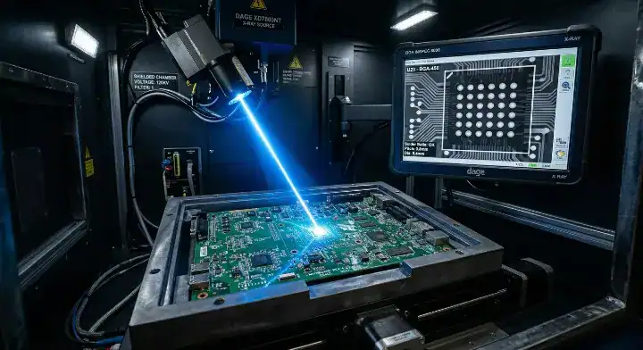
An X-ray inspection PCB assembly process relies on a focal tube firing photons through your circuit board to a digital detector, translating material density into a high-resolution grayscale image. Heavy elements like tin and lead solder block the rays and appear dark, while lighter materials like silicon, plastic, or FR4 appear translucent, allowing technicians to verify connections hidden entirely beneath component bodies.
The physics behind the machine dictate exactly what operators can see. Solder is extremely dense. When a manufacturer places a board inside an Automated X-Ray Inspection (AXI) chamber, the machine acts like a medical scanner. If an air bubble (void) exists inside a solid sphere of solder, the X-rays pass through the air gap easily, creating a bright white spot on the monitor right in the middle of a dark circle.
Now, here’s the part that surprises most customers… AXI machines do not just take a single static photo. Modern equipment features a multi-axis articulating sample platform. The engineer tilts the board up to 60 degrees while the X-ray is active. This oblique viewing angle allows them to look “under” the shadow of thick copper planes to inspect individual ball joints from the side.
The Core Components of AXI Systems
| System Component | Function | Direct Impact on Quality |
|---|---|---|
| X-Ray Focal Tube | Generates the photon beam | Higher kilovolts (kV) penetrate thicker multi-layer boards |
| Articulating Platform | Tilts and rotates the PCBA | Allows angled views to spot specific tear-drop shorts |
| Digital Detector | Captures the passing rays | Higher megapixel counts reveal sub-micron micro-cracks |
| Image Processing Software | Calculates grayscale density | Automatically flags void percentages over IPC limits |
The synergy between the articulating platform and the software dictates how fast the machine clears a board for shipping.
Bottom line: Never assume visual checks are enough; if your board utilizes packages with bottom-facing pads, photon penetration is the only physical way to verify the mechanical connection.
What Defects Can X-Ray Inspection Detect That AOI Cannot?
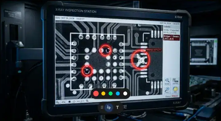
While standard cameras catch surface-level issues, X-ray inspection detects 100% of internal solder voids, Head-in-Pillow (HIP) mismatches, hidden bridging, and cold solder joints sitting directly underneath component packages. These internal faults cause intermittent thermal and electrical failures that easily pass a visual audit but immediately fail in the field.
Head-in-Pillow is the most notorious defect X-ray machines hunt down. It happens when the solder paste melts, and the component ball melts, but they never actually merge into a single joint. They rest against each other like a head resting on a pillow. Optically, they look connected. Electrically, they might even pass a bed-of-nails test. But the moment the device experiences thermal expansion or physical vibration, the connection breaks.
Factory Veteran View: The Problem: Clients using only visual checks experienced a 12% intermittent failure rate in the field due to Head-in-Pillow defects on heavy processing chips. Our Action: We mandated 3D X-ray profiling for the first 10 boards of every new BGA production run to optimize the reflow thermal profile before running the full batch. The Result: We dropped the field failure rate to 0.05% within one quarter, completely eliminating the HIP defect from the line.
Here’s where it gets real… You cannot diagnose these issues with a multimeter. Figuring out why PCBA testing is critical comes down to catching structural flaws before they leave the factory floor. X-ray provides the definitive proof.
Identifying Hidden Solder Faults
| Defect Type | X-Ray Detection? | AOI Detection? | Severity | Typical Cause |
|---|---|---|---|---|
| Head-in-Pillow (HIP) | Yes (with tilted view) | No | High | Component warpage during reflow |
| Hidden Solder Voids | Yes | No | Medium | Trapped outgassing from flux |
| Solder Bridges (BGA) | Yes | No | Critical | Excess paste or placement pressure |
| Missing Solder Balls | Yes | No | Critical | Dropped part before reflow |
| Tombstoning | Yes | Yes | Medium | Uneven thermal mass on pads |
AXI catches the structural integrity failures that cameras simply cannot access.
Bottom line: If your product operates in high-vibration or high-thermal stress environments, hidden voids will inevitably crack; X-ray is the only tool that prevents this failure before shipping.
Which Component Packages Require X-Ray Inspection?
Any Ball Grid Array (BGA) package requires mandatory X-ray validation, especially when the pitch drops below 0.5mm, while Quad Flat No-Lead (QFN) packages strongly require it to verify the critical center thermal pad. Engineers selecting components during the design phase must realize that choosing bottom-terminated packages instantly triggers secondary inspection costs.
A frequent oversight across hardware design forums is treating all surface-mount parts equally during cost estimation. If you place a standard SOIC chip on your board, the factory handles the inspection optically. The moment you drop a micro-BGA onto the layout, you force the assembly line to route that board through the lead-lined AXI chamber.
But here’s what most guides won’t tell you… QFNs are notorious for trapping gas. The large thermal pad directly under the IC is highly prone to voiding. If that voiding exceeds 30%, the chip cannot dissipate heat into the copper plane, leading to rapid thermal throttling. Understanding QFN package design means knowing that only an X-ray can verify your heat dissipation strategy actually worked on the line.
For high-density designs, BGA assembly is unavoidable, making AXI a non-negotiable step.
Package Inspection Requirements
| Component Package | Example Types | X-Ray Requirement | Primary Reason |
|---|---|---|---|
| Ball Grid Array | BGA, micro-BGA | Mandatory | 100% of connections are hidden |
| Chip Scale Package | CSP, WLCSP | Mandatory | Pitch is too fine for side-angle optics |
| Quad Flat No-Lead | QFN, DFN, LGA | Strongly Recommended | Center thermal pad voiding is invisible |
| Gull-Wing Leads | SOIC, QFP, TQFP | Not Required | All leads are 100% visible from above |
| Standard Passives | 0402, 0603, 0805 | Not Required | AOI easily catches surface anomalies |
Do not specify AXI for boards entirely populated by gull-wing leads and standard passives; you will pay for machine time you do not need.
Bottom line: If your bill of materials includes BGAs or QFNs processing high current, you must budget for automated X-ray validation to guarantee long-term thermal reliability.
X-Ray Inspection vs AOI: When Do You Need Which?
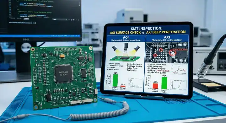
Automated Optical Inspection (AOI) provides rapid, low-cost surface defect detection, while X-ray inspection delivers thorough, higher-cost internal verification. They are strictly complementary systems; combining a rapid optical pass with a targeted X-ray scan on complex chips catches 98% of all manufacturing defects.
A common debate among engineers is whether high-end 3D AOI machines can replace AXI. The short answer is no. A telecom module client recently believed AOI was sufficient for their new product. During the ramp-up phase, the optical cameras successfully caught 95% of surface bridges and missing resistors. However, field units still overheated.
Factory Veteran View: The Problem: A client relied solely on optical checks, passing boards that later suffered aggressive thermal throttling in the field. Our Action: We ran their “passed” boards through our AXI machine and found a 15% void rate specifically under the QFN thermal pads that the cameras entirely missed. The Result: Implementing a dual AOI-then-X-ray workflow caught 100% of thermal voids, saving the client $22,000 in potential warranty replacements over six months.
The real question is: How do you sequence them? The standard industry protocol places AOI immediately after the reflow oven to catch gross errors fast. The board only moves to the X-ray station if the optical scan passes. Learning how first article inspection compares to AOI helps you structure your testing pipeline efficiently.
AOI and AXI Capability Comparison
| Feature | Automated Optical (AOI) | Automated X-Ray (AXI) |
|---|---|---|
| Core Technology | High-resolution cameras & lasers | Photon penetration & density tracking |
| Speed per Board | Very Fast (10–30 seconds) | Slow (2–5 minutes) |
| Cost Impact | Low (Usually included in base price) | High (Adds specific machine time fees) |
| Best Used For | Missing parts, wrong orientation, surface bridges | Hidden voids, HIP defects, BGA ball alignment |
| Major Limitation | Cannot see under physical component bodies | Cannot read part numbers or text on components |
Using AOI for speed and AXI for depth creates a foolproof quality control net.
Bottom line: Always run AOI on 100% of your boards to catch cheap surface errors fast, but strictly reserve X-ray inspection for validating the hidden joints under your high-value ICs.
2D vs 3D X-Ray Inspection: What Is the Difference and Which Should You Specify?
2D X-ray systems generate a single top-down image that is fast and cost-effective for basic void calculations, whereas 3D X-ray (CT scanning) compiles multiple angled slices to pinpoint the exact vertical depth of a defect within a multi-layer board. You should specify 3D X-ray when inspecting double-sided BGA assemblies where top and bottom components overlap.
If your board has a BGA mounted directly above another BGA on the opposite side of the PCB, a 2D X-ray is useless. The 2D image will compress both chips into a single flat picture, creating a massive, unreadable black blob of overlapping solder balls.
So what does this actually mean for your budget? 3D X-ray, also known as Computed Tomography (CT), requires advanced software to reconstruct the slices, making it significantly slower and more expensive. The machine rotates the detector and the source around the board, taking hundreds of images to build a 3D model.
For standard single-sided designs, an angled 2D system (often called 2.5D) provides plenty of diagnostic power at a fraction of the cost.
Dimensional Scanning Breakdown
| Technology | Resolution / Depth | Speed | Ideal Application Scenario |
|---|---|---|---|
| 2D AXI | Flat projection, no depth data | Fast | Single-sided boards, basic void percentage checks |
| 2.5D AXI | Oblique angled flat projection | Medium | Spotting Head-in-Pillow defects on single-sided BGAs |
| 3D AXI (CT) | Full cross-sectional depth slices | Slow | Double-sided BGAs, package-on-package (PoP) |
Do not demand 3D CT scanning unless your board stack-up physically requires slicing to separate overlapping component shadows.
Bottom line: Specify standard 2D or 2.5D X-ray to save money on 90% of typical designs, but mandate full 3D CT scanning if you have dense bottom-terminated components on both sides of the board.
Which Industries and IPC Classes Require Mandatory X-Ray Inspection?
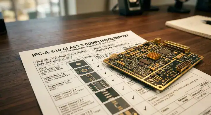
Aerospace, medical, and automotive industries legally require 100% X-ray inspection to comply with IPC-A-610 Class 3 standards, which strictly limits BGA voiding to less than 25% of the solder ball volume. If your product operates in an environment where failure causes injury or massive financial loss, this inspection is not optional—it is a regulatory mandate.
When you classify your project, the IPC class dictates the factory’s workflow. Class 1 (general electronic products) and Class 2 (dedicated service electronics) allow some leeway. Manufacturers usually run a sampling strategy for these classes, X-raying maybe 1 in every 10 boards.
Want the honest answer? If you demand Class 3, the factory must document every single joint. The IPC-7095 standard specifically addresses BGA design and assembly implementation. It clearly defines the acceptable sizes and locations of solder voids. Understanding IPC standards for PCB reliability forces you to align your budget with your compliance requirements.
Industry Compliance Standards
| Target Industry | Applicable Standard | X-Ray Requirement Level | Maximum Acceptable Voiding |
|---|---|---|---|
| Aerospace & Defense | IPC-A-610 Class 3 | 100% Mandatory | Under 25% |
| Medical Devices | ISO 13485 / Class 3 | 100% Mandatory | Under 25% (Documented) |
| Automotive | IATF 16949 / Class 3 | 100% Mandatory | Strict adherence to IPC-7095 |
| Telecom Infrastructure | IPC-A-610 Class 2 | Sampling Recommended | Typically 30% |
| Consumer Electronics | IPC-A-610 Class 1 | Optional / Prototyping only | Often up to 35% |
Factories must keep the digital X-ray image logs on file for medical and aerospace clients for years to prove compliance during FDA or FAA audits.
Bottom line: If your hardware requires Class 3 certification, you must explicitly state that 100% X-ray inspection is required on the RFQ, as it legally changes the manufacturing timeline and documentation process.
How Does X-Ray Inspection Affect Your PCB Assembly Cost and Lead Time?
Adding X-ray inspection typically increases your per-board assembly cost by $0.50 to $2.00 and extends production lead times by 1 to 2 days, strictly depending on whether you require a 100% scan rate or a statistical sampling approach. Because AXI relies on skilled operator time and slow machine cycles, it directly impacts the final invoice of any BGA-heavy project.
Engineers routinely underestimate how component choices impact manufacturing fees. A startup recently complained about a $4.50 per board inspection fee on a simple consumer device. The cost driver was a single 0.4mm micro-BGA that forced the entire batch through the AXI bottleneck.
Factory Veteran View: The Problem: A client was paying premium inspection fees because their designer utilized an unnecessary micro-BGA on a low-speed IoT device. Our Action: We reviewed the BOM during the DFM stage and suggested swapping the micro-BGA for an electrically equivalent LQFP package that could be verified entirely via standard optical cameras. The Result: The client eliminated the X-ray requirement entirely, dropping their per-board assembly cost by $1.85 and cutting lead time by 24 hours.
Here is the reality… You can heavily mitigate these costs using a Golden Sample baseline. The factory runs the first 5 boards through 100% X-ray. Once the thermal profile is perfected and the baseline images are locked, they switch to inspecting 1 in 20 boards for the rest of the production run.
X-Ray Cost Impact Breakdown
| Production Volume | Inspection Strategy | Estimated Cost Impact | Cycle Time Impact |
|---|---|---|---|
| Prototypes (5–10 units) | 100% Scan | $30 – $80 flat NRE fee | Adds 12 hours |
| Low Volume (100+ units) | 100% Scan | $1.50 – $3.00 per board | Adds 1 – 2 days |
| Low Volume (100+ units) | Sampling (1 in 10) | $0.20 – $0.50 per board | Negligible |
| Mass Production (10k+) | Golden Baseline + Sampling | Included in unit cost | Built into line flow |
Selecting the right inspection ratio based on your product’s risk profile keeps your budget intact while maintaining reliability.
Bottom line: To save money in the design stage, swap unnecessary BGAs for leaded packages; if BGAs are required, use a 100% scan for prototypes and drop to a 10% sampling rate for mass production.
How to Specify X-Ray Inspection Requirements When Ordering PCB Assembly?
You specify your X-ray requirements by explicitly listing the inspection percentage rate, defining the acceptable void limit under IPC standards, and requesting image archival directly in your manufacturing Request for Quote (RFQ). Failing to write these terms into your initial PO means the factory will default to their standard, undocumented visual checks.
Many purchasing managers simply write “Inspect boards thoroughly” on their orders. The factory interprets this as standard AOI. If you need X-ray, you must ask for it using precise engineering language.
So what does this actually look like on paper? Your assembly drawing notes should explicitly state: “100% AXI required on U4 and U7. Voiding must not exceed 25% per IPC-7095. Provide digital image report with shipment.” This leaves zero room for factory interpretation and locks the inspection cost into the quoted unit price.
RFQ Specification Checklist
| Specification Item | What to Write in the RFQ | Why It Protects You |
|---|---|---|
| Inspection Ratio | “100% X-ray on first 10 boards, 15% sampling thereafter” | Prevents you from paying 100% rates on a 5,000 unit run |
| Targeted Components | “Focus AXI on all BGA and QFN packages only” | Speeds up machine time by skipping irrelevant passive parts |
| Acceptance Standard | “Adhere to IPC-A-610 Class 2 voiding limits” | Sets a legal benchmark for rejecting poorly soldered boards |
| Deliverables | “Include digital X-ray report and baseline images” | Gives you proof of compliance for your own QA records |
If a contract manufacturer pushes back on providing digital image reports, they likely outsource their X-ray work to a third-party lab, which adds hidden delays.
Bottom line: Write your exact AXI sampling percentage and IPC voiding limits directly into your assembly drawing notes so the factory legally commits to the validation standard before you pay the invoice.
Guessing whether your high-density chips are properly soldered shouldn’t keep you awake at night—now you have the framework to demand the right inspection level for your specific packages. At QueenEMS, we offer full turnkey services with completely transparent pricing, providing a free DFM/DFA engineering review on every single order. With our 3D AOI and X-Ray inspection standard on every BGA joint, you achieve a 99.7% first-pass yield rate that scales seamlessly from prototype to mass production. We believe every hardware team deserves a manufacturing partner who explains their quality control processes, not hides them. Contact us today to get a detailed quote that includes exactly the testing your board needs.
Written by the QueenEMS Engineering Team
FAQ
1. Does my simple 2-layer board with standard SMD components need X-ray inspection? No, it does not. If your board only uses gull-wing ICs (like SOIC) and standard passives (like 0603 or 0805 resistors), standard optical cameras can easily see 100% of the solder joints. You will waste money requesting an X-ray scan for this type of design. Upload your BOM for a free DFM check and we will tell you exactly which inspection method fits your components.
2. Can an X-ray machine tell if the factory installed the wrong value resistor? No, it absolutely cannot. AXI machines measure material density, not electrical resistance or printed text. A 10k ohm resistor and a 100k ohm resistor look exactly identical in an X-ray image. To catch wrong component values, you must rely on AOI to read the top markings or use functional testing. Request a free first-article inspection on your first order to verify your components are placed perfectly.
3. Will the X-ray inspection damage my sensitive memory chips or microcontrollers? No, the inspection is completely non-destructive. The photon dose used in standard electronic assembly scanning is incredibly low and exposure time is very brief. It will not erase firmware, corrupt flash memory, or degrade the silicon in your microcontrollers. Get a transparent quote within 24 hours to see how we safely handle your sensitive hardware.
Upload your files today · Free DFM check before production · Ship worldwide
Get your PCB prototypes in as fast as 24 hours. We handle FR4, Rogers, and Flex up to 60 layers — free prototypes for 2–4 layer boards, no minimum order.
Just upload your Gerber + BOM — we source every part, assemble, and inspect (AOI + X‑Ray) so you don't have to chase suppliers. Boards ship in as fast as 24 hours.