
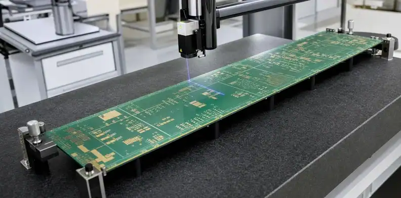
Quick Answer: Large PCB warpage control begins before fabrication by defining the flatness risk, using a mechanically balanced stack-up, reviewing copper distribution, selecting a suitable thickness and agreeing how bow and twist will be measured. Bare-board flatness alone is not enough when the assembly contains BGAs, long connectors or heavy components. The release package should connect design controls, supplier evidence and first-article assembly checks.
Large PCB warpage control is most effective while the stack-up, copper and mounting scheme can still change. Once laminate is pressed and components are committed, the available actions become sorting, special fixturing, conditional assembly or replacement. Those actions protect a schedule; they do not remove the stress built into the design.
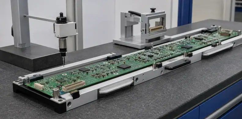
The practical objective is not a perfectly flat mathematical plane. It is a board that stays within an agreed measurement rule and remains compatible with solder paste printing, placement, reflow, test and enclosure fit. A useful review therefore follows the board from layout through first-article assembly instead of treating warpage as a final cosmetic inspection.
Table of Contents
- Define what large PCB warpage control must prevent
- Balance the structure around its centerline
- Review copper by layer and by region
- Choose thickness from the mechanical system
- Control cutouts, connectors and component mass
- Agree measurement and evidence before the PO
- Verify the board through assembly
- Release production with a disposition path
Define what large PCB warpage control must prevent
Warpage becomes a manufacturing problem when it changes contact, alignment, support or mechanical fit. Begin by identifying the first operation or interface that would fail, because that determines the appropriate control and evidence.
During solder paste printing, a bowed board can prevent consistent contact between the stencil and pads. During placement, twist changes local surface height. Reflow can expose residual stress as the resin system and copper heat unevenly. A connector at one end of a long board may align in the free state but move after the board is fastened into an enclosure.
List the sensitive zones on the mechanical drawing or assembly notes:
- BGAs, land-grid arrays and other bottom-terminated components;
- long or paired board-to-board connectors;
- card-edge contacts and guide rails;
- press-fit fields and large through-hole connectors;
- test fixture support and probe areas;
- screw locations that can force the board into shape;
- large cutouts or narrow webs;
- heavy transformers, shields, heatsinks or power parts.
The board does not need the same flatness margin everywhere. A raised corner far from circuitry may matter less than local movement under a fine-pitch package. Keep the acceptance rule simple enough to inspect, then add local first-article checks where the assembly risk is concentrated.
Use the PCB bow and twist specification article for the measurement language. This article focuses on preventing scale-dependent distortion before the released design enters fabrication.
Balance the structure around its centerline
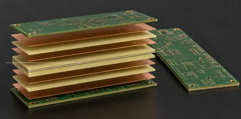
A numerically even layer count is not the same as a mechanically balanced stack-up. Copper thickness, dielectric construction, resin distribution and material type should be reviewed as mirrored relationships around the board’s centerline.
A six-layer stack can be electrically logical and mechanically weak if heavy copper sits mainly above the centerline, if dielectric thicknesses differ sharply between the two halves or if one side contains a material with different expansion behavior. Heating and cooling then create unequal strain through the thickness. Over a large span, that strain produces more visible curvature than it would on a compact board.
The review should compare paired layers, core and prepreg arrangement, finished copper, resin demand and any mixed-material construction. A symmetric drawing does not guarantee that dense and open copper patterns are symmetric, so stack-up review must be followed by artwork review.
| Construction element | Warpage question | Release record |
|---|---|---|
| Mirrored layer pair | Are copper weight and density mechanically comparable? | Layer-pair density review |
| Core and prepreg | Are dielectric thickness and resin demand balanced? | Supplier production stack-up |
| Mixed material | Do expansion and cure behaviors remain compatible? | Approved material disposition |
| Heavy copper region | Is local stiffness offset or supported? | Artwork and mechanical review |
Avoid changing the supplier stack only to preserve a desired overall thickness without checking the mechanical result. If a prepreg is replaced, a core is changed or copper is redistributed, confirm that impedance, resin fill, finished thickness and balance remain acceptable. The supplier stack-up signoff process provides a useful approval record, while the PCB stack-up design guide covers the broader electrical choices.
The design release should state who may adjust the construction. Routine material builds within an approved stack may belong to the fabricator; layer-order changes, dielectric substitutions or copper-weight changes should return to engineering.
Stackup rule: Release the build only when mirrored construction and supplier adjustment authority are both documented.
Review copper by layer and by region
Copper balance must be checked both across mirrored layers and across the board area. Two layers can have similar total copper percentages while still concentrating stiffness and thermal mass in opposite corners.
Start with a visual density map for each layer. Compare the top and bottom outer layers, then mirrored inner pairs. Look for large planes on only one side, broad copper-free zones, dense power regions, long bus bars and abrupt transitions between open and filled artwork. A single total percentage can hide all of these local conditions.
Do not add floating copper merely to improve a chart. Added features need an electrical and manufacturing disposition: connected fill, approved thieving or another CAM feature agreed with the supplier. Uncontrolled floating islands may create unintended coupling, isolation questions or drawing conflicts. The QueenEMS article on PCB copper balance and CAM approval defines how to document that authority.
Solid versus hatched copper is also not a universal warpage rule. Solid planes support return paths, shielding and current flow; a hatch changes electrical and thermal behavior. When a forum recommends replacing every large plane with mesh, treat that as a prompt for engineering review, not a design standard. The correct result may be a mirrored plane, local thieving outside the functional circuit or a revised stack-up.
Record protected areas where the fabricator may not add copper, such as antennas, high-voltage isolation regions, controlled-impedance channels and optical openings. If process thieving is allowed elsewhere, define clearance and approval expectations using the copper thieving requirement guide.
Choose thickness from the mechanical system
Board thickness affects stiffness, but the correct value also depends on connectors, impedance, drilling, weight and enclosure geometry. Increasing thickness only to fight warpage can move the problem into another interface.
A thicker large board generally resists bending more than a thinner board of the same material and outline. It may also require longer press-fit pins, different connector tails, adjusted edge-card geometry or a different via aspect ratio. Added thickness increases mass and can change the thermal response during assembly.
The mechanical team should review the free span between supports, mounting method, board orientation and expected vibration. A horizontal board supported only at its edges behaves differently from a vertical backplane held in card guides. A large cutout can reduce local stiffness even when the nominal thickness appears generous.
Use the PCB thickness selection process to capture connector and fit constraints. For warpage control, add three questions: What span remains unsupported? Which regions carry high mass? Will the board be measured in a free state or installed state?
An engineering drawing may need both finished-thickness tolerance and a separate flatness requirement. Thickness tolerance controls mating and construction; flatness controls shape. Combining them into one vague note leaves the supplier unsure which condition governs rejection.
Mechanical call: Choose thickness from connector, support and via constraints, then specify flatness as a separate acceptance condition.
Control cutouts, connectors and component mass
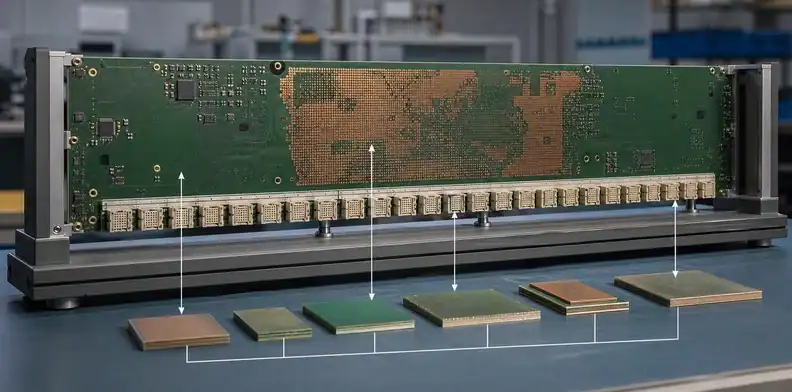
Large openings, narrow bridges and uneven component mass create local stiffness and heating differences that a symmetric stack-up cannot solve by itself. Review them with the mechanical and assembly models visible.
A central cutout can turn one wide plate into a flexible ring. Long slots can create narrow beams that twist during handling. Dense connector fields near one edge may stiffen the assembled board while the opposite side remains flexible. These features should be marked during DFM review rather than discovered when the first board is lifted from its carrier.
Datum strategy matters as the distance between interfaces grows. If connectors at opposite ends are dimensioned through a chain of intermediate features, small tolerances can accumulate. Define functional datums that represent the enclosure or mating parts, then ask the fabricator how hole, pattern and routed-outline registration will be controlled to them.
Component distribution adds another layer. A group of heavy power devices or shields can create a cold region during reflow and a high local load afterward. Moving parts is not always electrically acceptable, but the risk can be managed with thermal profiling, local support or a carrier. The board drawing should not attempt to prescribe proprietary oven settings; the assembly package should identify high-mass zones and components with restricted process windows.
For release, combine the board data with the assembly drawing. The DFM review before placing a PO is the correct stage to resolve large cutouts, tooling margins, datum questions and support needs.
Agree measurement and evidence before the PO
A flatness limit is only enforceable when the condition, method, sample and evidence are defined. Writing “no warpage allowed” creates a dispute because every real board has some measurable deviation.
IPC-TM-650 Method 2.4.22 defines bow and twist measurements; it does not assign the product acceptance limit. The automotive addendum IPC-6012EA applies when the procurement documentation invokes it and is used with IPC-6012E. Procurement requirements take precedence. Its Section 3.4.3 specifies a 0.75% maximum when no different limit is specified and the board is designed in accordance with IPC-2221; pallet-array requirements are AABUS, meaning as agreed between user and supplier. The addendum also requires two 260 °C reflow preconditioning cycles before assessment. Those automotive conditions are not a default rule for every large PCB. Confirm the applicable revision, board condition and acceptance rule in the drawing or purchase order; unresolved inputs require written customer-supplier agreement before production.
Build an evidence note with these fields:
| Field | Required decision |
|---|---|
| Condition | Single board or panel; before or after specified thermal exposure |
| Reference | Named measurement method and datum surface |
| Limit | Drawing value or agreed standard requirement |
| Sample | Qualification, lot sample or 100% check where justified |
| Record | Actual gap, calculated percentage, board identity and setup photo |
| Escalation | Hold point and approval owner for borderline results |
For large boards, state which length, width or diagonal controls the calculation. Also define whether temporary flex while handling is excluded by allowing the board to rest in the agreed condition before measurement.
Send the stack-up, copper-density plots, outline, thickness and flatness requirement for a warpage-risk review. The useful return is a list of design controls, unresolved assumptions and proposed evidence—not a promise that any board will be perfectly flat.
Evidence check: A percentage limit is actionable only when board condition, test method, sample plan and disposition owner are named.
Verify the board through assembly
Incoming flatness does not prove that the populated board will remain compatible with printing, reflow and mechanical assembly. Verification should follow the risk through the first build.
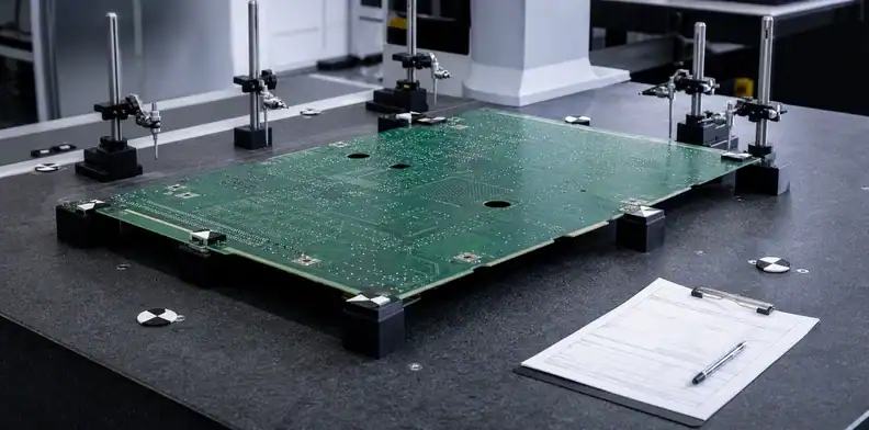
At receiving, record board revision, lot, packaging condition and measured free-state result. Before production, the assembler should confirm stencil support, conveyor orientation, carrier need and component thermal-mass distribution. If the board contains BGAs or long connectors, identify the inspection or fit check that will confirm the chosen control worked.
Reflow profiling should measure representative hot and cold regions rather than one convenient location. Nexperia’s reflow application note explains the need to bring cold and hot spots into a workable soldering window without exceeding component or board limits. A large board does not create a new universal profile; it increases the value of board-specific measurement.
After first-article reflow, compare the board with the incoming condition. A board that was already outside the agreed limit should not be blamed on assembly without evidence. A board that changed materially through reflow needs a joint review of moisture, support, thermal distribution and built-in stress.
Inspection evidence can include flatness measurements, paste inspection in sensitive regions, X-ray where package risk justifies it, connector fit and fixture behavior. The PCB quality documents before shipment help tie those results to the production lot.
Release production with a disposition path
Production control needs a defined response for pass, borderline and fail conditions. Without a disposition path, schedule pressure will create a new rule after the boards arrive.
Use three outcomes. A board within the agreed condition is released with its evidence. A borderline board may receive conditional release for a controlled first-article assembly, with the approver and inspection result recorded. A board outside the limit near a critical package, connector or enclosure interface remains on hold until replacement, sorting or a documented engineering concession is approved.
Do not flatten suspect boards with uncontrolled heating or mechanical force. Such action can damage copper, vias, laminate or assembled joints even when the board looks improved afterward. Any recovery method must be part of a qualified process with acceptance evidence.
For repeat builds, preserve the stack-up revision, laminate, copper distribution, panel orientation, flatness data and assembly support method. Revalidate the risk if a revision adds a large plane, moves a connector, changes thickness or modifies a cutout.
For a warpage-specific quotation, send QueenEMS the released Gerber/ODB++ package, stack-up, copper weights, mechanical drawing, flatness requirement, quantities and assembly risk zones. The engineering response can return a buildability disposition, required DFM changes and proposed inspection scope tied to the actual design.
Bottom line: Production release requires both bare-board flatness evidence and first-article confirmation at the interfaces that can fail.
FAQ
Can a warped large PCB be straightened after fabrication?
Do not assume so. Uncontrolled heat or force can create hidden damage. First measure the condition, identify whether the board is before or after assembly, and obtain a documented supplier disposition.
Does a symmetric stack-up guarantee a flat board?
No. Layer order can be symmetric while local copper, resin demand, cutouts, component mass or thermal history remains unbalanced.
Should every large copper pour be hatched?
No. Hatching changes electrical, thermal and shielding behavior. Review mirrored copper, functional requirements and approved thieving before changing a plane.
When should flatness be measured?
Measure at the stage that supports the decision: outgoing bare-board inspection, incoming assembly inspection and after first-article reflow when thermal movement affects critical components or fit.
What should purchasing put in the RFQ?
State the board condition, measurement method, applicable limit, sampling requirement, evidence format and approval path for borderline results.
Sources
- IPC-6012EA Automotive Addendum: Scope and Table 1 Excerpt
- Nexperia AN10365: Surface Mount Reflow Soldering
Written by the QueenEMS Engineering Team
Upload your files today · Free DFM check before production · Ship worldwide
Get your PCB prototypes in as fast as 24 hours. We handle FR4, Rogers, and hybrid boards up to 40 layers in volume production, with advanced builds subject to engineering review — free prototypes for 2–4 layer FR-4 boards, no minimum order.
Just upload your Gerber + BOM — we source every part, assemble, and inspect (AOI + X‑Ray) so you don't have to chase suppliers. Boards ship in as fast as 24 hours.