
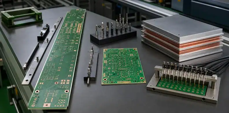
Quick Answer: Maximum PCB size is set by the smallest usable process window in the complete manufacturing route, not by laminate sheet dimensions alone. QueenEMS publishes project-review envelopes up to 2000 × 600 mm for 1–2 layers and 1400 × 540 mm for 4–10 layers. Three-layer, 11-layer and 12-or-more-layer requests require project-specific stack-up review rather than inheriting a published row automatically. Treat every maximum as conditional on material, thickness, copper, finish, special processes and test method.
Maximum PCB size looks like a simple length-and-width question until a real quotation begins. A buyer may find a large laminate sheet, see a drilling table with generous travel and assume the finished board will fit. The manufacturer still has to move that same panel through every required operation without losing registration, flatness or test access.
That is why a useful answer starts with the complete process route. A two-layer industrial bus board and a ten-layer controlled-impedance backplane may have the same outline, yet they do not create the same manufacturing window. The second board adds inner-layer imaging, lamination movement, more registration relationships and a more demanding inspection plan.
Table of Contents
- Why maximum PCB size is a process-chain decision
- Layer count changes the usable envelope
- Finished size and panel size are different
- Materials and copper can reduce the limit
- Special processes create additional bottlenecks
- Assembly may impose a smaller maximum
- Build a layer-dependent feasibility package
- Turn the answer into a controlled quotation
Why maximum PCB size is a process-chain decision
The governing maximum is the smallest qualified window among every process the job needs. A large panel may fit one machine and still fail the route because a later operation has a smaller working field, restricted tooling margin or unsupported handling condition.
Start with the actual sequence: material cutting, inner-layer imaging where applicable, lamination, drilling, plating, outer-layer imaging, solder mask, surface finish, profiling, electrical test and final inspection. Each step has a physical field and a process margin. The usable area is normally smaller than the machine’s advertised travel because the panel may need tooling holes, plating contacts, registration targets, edge clearance or gripping space.
| Process gate | Size question | Required evidence |
|---|---|---|
| Imaging and lamination | Can all layers stay registered across the usable field? | Approved production stack and registration route |
| Drilling and profiling | Do travel, tooling and support accept the panel? | Panel drawing with tooling and finished outline |
| Finish and test | Can the full board pass the selected line and test field? | Route-specific finish and electrical-test disposition |
| Assembly | Do printer, placement, reflow and inspection accept the carrier? | Complete PCBA equipment-route review |
This distinction matters during sourcing. A capability table that lists only “maximum panel size” does not confirm the maximum finished board. It may describe an early operation rather than the entire route. Ask which operation controls the quoted limit and whether the number applies to a single finished board, a production panel or incoming raw material.
QueenEMS publishes the standard large-board envelope on its large format PCB manufacturing page, but the table is a starting point rather than permission to release any design at the listed outline. The construction still has to pass the PCB manufacturer capability review for the required material and features.
A practical feasibility answer should name four items: the accepted finished outline, the production panel or single-board route, the controlling operation and any restrictions that remain open. Without those four items, “yes, we can make it” is not yet a release decision.
Layer count changes the usable envelope
More layers add process relationships that must remain aligned across a larger area. The issue is not that copper layers consume length or width; the issue is that multilayer construction adds imaging, lamination and registration risk before the finished board reaches drilling and routing.
A one- or two-layer board avoids multilayer lamination. Its copper features are formed on the external faces, and the main dimensional relationships are between artwork, holes and outline. A multilayer board adds individually imaged inner layers, oxide or other bond preparation, cores and prepregs, a lamination cycle, buried targets and post-lamination registration. Material movement that would be modest on a smaller panel becomes more visible over a long span.
Layer count alone is still not enough to quote. Two six-layer boards may require different envelopes because one uses a conventional through-hole structure while the other adds sequential lamination, controlled-depth routing or tight impedance registration. The PCB stack-up design guide explains the electrical and construction choices; the maximum-size review adds the question of whether that stack can be processed over the full outline.
QueenEMS publishes review envelopes of 2000 × 600 mm for 1–2 layer finished boards and 1400 × 540 mm for 4–10 layers. These published figures are starting points for project review, not approval of a particular construction or an assembly-line limit. Three-layer and 11-layer designs do not inherit either published row automatically; they need stack-up review, and engineering may propose a balanced even-layer construction before confirming size. Boards with 12 or more layers also require project-specific consultation. Material, thickness, copper, finish, special processes and test coverage can reduce the feasible outline.
The project response should identify the finished outline, material system, finished thickness, copper construction and electrical-test route that the quoted size covers. It should also name the operation that sets the limit and list any trial or customer approval still required. Keep that response with the approved stack-up. A change from a conventional through-hole build to a different via or lamination route requires a new size disposition.
| Layer count | Maximum finished-board envelope | Release condition |
|---|---|---|
| 1–2 layers | 2000 × 600 mm | Written engineering confirmation |
| 4–10 layers | 1400 × 540 mm | Written engineering confirmation |
| 12+ layers | Confirm by stack-up and process | Project-specific consultation |
The buyer should therefore avoid writing only “maximum size required” in an email. State the layer count, proposed stack-up, finished thickness and whether the design contains blind or buried vias. Those details turn a headline number into a manufacturing answer.
Decision point: Approve an outline only after the layer count and complete process route are named in the same feasibility record.
Finished size and panel size are different
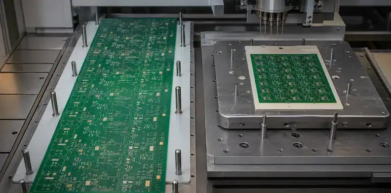
Finished-board size describes the delivered outline; production-panel size describes the temporary manufacturing format. Confusing them can remove tooling room, invalidate an array or create a quotation that cannot survive CAM review.
A very large PCB may run as one board on one panel. Even then, the manufacturing panel can need extra material outside the final outline for registration targets, process coupons, plating contacts, rails or handling. If a finished board approaches the quoted machine field, the process may require a special edge strategy rather than an ordinary panel border.
For smaller products, panelization is often discussed as a way to improve assembly throughput. With oversized products, panel planning is more often about support and process access. The supplier may need to decide whether the board remains in a framed panel through solder mask or routing, whether rails are removed before test and which edge can carry tooling features.
The fabrication drawing should identify the finished outline clearly and keep customer-requested rails separate from supplier-added process material. If the customer supplies an array, confirm whether its outside dimensions are treated as the production panel. The PCB panel drawing approval process is useful when rails, breakaways or coupons are customer-controlled.
This is also why a CAD file that fits within a nominal rectangle is not proof of manufacturability. The CAM team needs room to build the route that the drawing and acceptance criteria require.
Materials and copper can reduce the limit
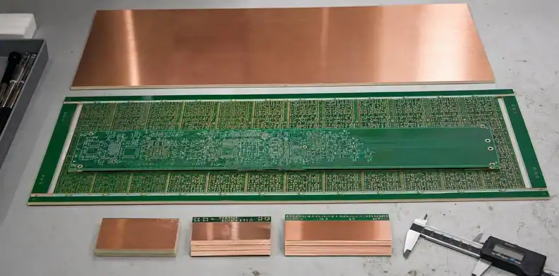
The usable maximum can shrink when the selected material or copper weight cannot follow the same qualified route as standard FR-4. Sheet availability, press format, resin flow, etching and dimensional stability all have to match the outline.
Start with material identity. “FR-4” is a family description, not a complete laminate specification. A buyer may require a named material, Tg range, loss performance, halogen-free formulation or high-temperature behavior. The manufacturer must confirm that the exact core and prepreg family is available in the required sheet and thickness combinations. Substituting another laminate to obtain a larger sheet may change impedance, thermal behavior or customer qualification.
Copper weight changes more than current capacity. Heavy copper affects image compensation, etching, plating distribution and resin fill around features. It can also increase structural imbalance when copper density is concentrated on one side or one region. The heavy copper PCB design requirements should be reviewed together with the large-board envelope rather than applied after the size is approved.
Finished thickness can help mechanical stiffness, but it also changes drilling, routing, connector fit and press construction. Very thin large boards may need additional process support; very thick boards may exceed an operation’s handling or tooling condition. Review the PCB board thickness selection before treating thickness as a simple anti-warp correction.
For quotation, provide the laminate brand and model when it is mandatory. If equivalent material is allowed, state the electrical, thermal, flammability and dimensional properties that must be preserved. That lets the supplier distinguish a real substitution boundary from an informal preference.
Material rule: A larger raw sheet does not enlarge the qualified board envelope unless the specified laminate and copper construction pass every downstream operation.
Special processes create additional bottlenecks
Advanced features do not automatically inherit the maximum size of a standard through-hole board. Every added process needs its own usable field, registration plan and inspection route.
Controlled impedance is a common example. A long board may carry long channels, but the supplier still needs a qualified stack-up, finished trace geometry and coupon or test plan. If the production panel cannot accommodate the agreed coupon, the impedance evidence may require another approach. Use the controlled-impedance specification guide to define the requirement before asking whether the maximum outline remains available.
Blind and buried vias can introduce sequential lamination or additional drilling stages. Resin-filled vias, controlled-depth routing, edge plating, countersinks, long slots and selective finishes can each introduce a smaller machine field or a handling restriction. Surface finish matters as well: a board that fits imaging and drilling still has to pass the selected finish line without unsupported contact or uneven processing.
Electrical testing is another frequent late surprise. A board may fit fabrication equipment but exceed the convenient field of a standard fixture or flying-probe setup. That does not automatically make the design impossible, but the test method and coverage must be confirmed during quotation. The buyer should state whether 100% net test, test voltage, isolation expectations or a customer-specific report is required.
The safest rule is to ask for a route-specific answer. Do not combine the maximum size from one table with the minimum feature from another table and assume both extremes can run together. A capability corner needs an engineering review because maximum dimensions, fine features, heavy copper and special structures often compete for process margin.
Assembly may impose a smaller maximum
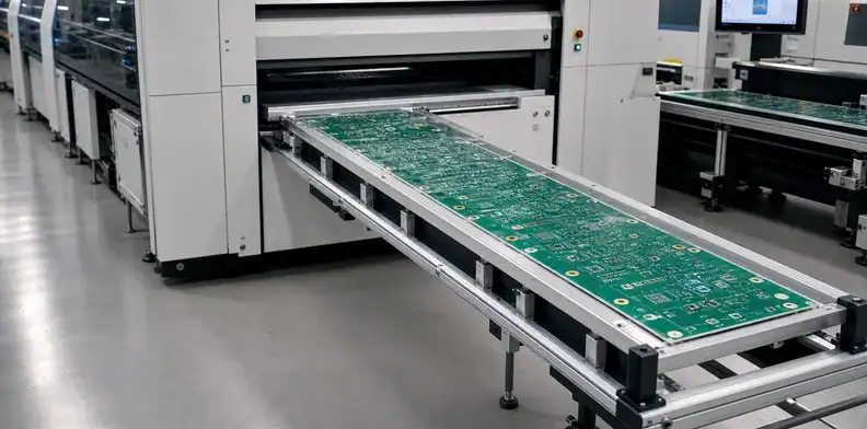
Bare-board fabrication and PCB assembly have separate maximum-size limits. Stencil printing, solder paste inspection, placement, conveyor transport, reflow, automated optical inspection and test must all accept the populated board or its carrier.
This separation matters because the bare board may be fabricated as a single supported panel while the SMT line expects a different width, edge rail or conveyor orientation. Component height and weight can create further restrictions. A long board with heavy connectors may fit the conveyor but need support to prevent sag during printing or reflow.
Ask the assembler to review the board outline, thickness, mass, component map, placement sides, largest components, tooling edges and preferred travel direction. A generic statement that the facility provides SMT does not confirm the full route. The large format PCB manufacturing and assembly review page should be used as the commercial handoff, while the exact equipment window is confirmed against the job.
Nexperia’s surface-mount reflow guidance shows why a board-specific thermal profile matters: hot and cold regions must both reach a workable soldering window without overheating sensitive locations. On a large assembly, thermal mass can vary significantly across the area. The process review therefore needs component and copper distribution, not only length and width.
The sourcing decision should record two answers: maximum bare-board construction and maximum assembled route. If they differ, the team can change orientation, rails, carrier, assembly sequence or system architecture before committing material.
Route check: Treat the smaller of the approved fabrication and assembly envelopes as the maximum deliverable PCBA size.
Build a layer-dependent feasibility package
A buildable size review needs enough data to reconstruct the complete route. Sending only a board outline invites a provisional answer that may change when the stack-up or finish appears.
Prepare one controlled package containing:
- Gerber or ODB++ data with a clear outline layer;
- NC drill and route information;
- fabrication drawing with finished dimensions and tolerances;
- layer count and proposed stack-up;
- laminate brand/model or permitted equivalency boundary;
- finished thickness and tolerance;
- inner and outer copper weights;
- surface finish and special processes;
- impedance, electrical test and inspection requirements;
- prototype and production quantities;
- assembly scope, when the same project includes PCBA;
- target destination and required delivery condition.
The package should identify one revision across every file. A board drawing from revision B and Gerber data from revision C can produce a false size conflict even when each file looks valid alone. The PCB fabrication quote file requirements provide the general file-control background; large boards add process-window and support questions.
Mark uncertain items honestly. A proposed material is different from a frozen material. A target thickness is different from a connector-controlled thickness. A preliminary quantity is different from a released production schedule. Suppliers can quote open items, but the assumptions must remain visible.
At this point a contextual engineering review is useful. Send the outline, layer count, stack-up and material requirement for a size-route assessment; the return should identify the standard or custom envelope, limiting operation and open conditions rather than only repeat a maximum number.
Turn the answer into a controlled quotation
The final quotation should preserve the construction that made the size feasible. If a key assumption changes, the size approval needs to be reviewed again instead of silently carried into the next revision.
Create a short capability record beside the commercial quote. It should state the finished outline, production format, layer count, material, thickness, copper, finish, special processes, test route and assembly inclusion. Record any supplier CAM authority, such as adding process copper, modifying external rails or applying scale compensation within an agreed window.
Compare suppliers on the same package. One quote may assume generic FR-4 and standard electrical test; another may include the named laminate, flatness evidence and protected packaging. The lower price is not comparable until the assumptions match. The DFM review before purchase order helps turn unresolved engineering comments into a release decision.
For repeat orders, do not treat the previous maximum-size approval as permanent if the revision changes copper balance, thickness, laminate, surface finish or panel format. A small electrical edit may have no effect, while a revised connector position or large copper plane can alter registration and flatness risk.
For a project-specific quotation, send QueenEMS the controlled fabrication package, quantity breaks and any assembly requirements. The engineering response can return a layer-dependent size disposition, major DFM questions, inspection scope and quotation based on the same documented assumptions.
Record rule: Reopen the size approval whenever the stack-up, material, copper, finish, test method or assembly route changes.
FAQ
Is there one universal maximum PCB size?
No. The usable maximum is the smallest qualified window in the required fabrication, finishing, testing and assembly route. Layer count, material, copper, thickness and special processes can all change it.
Can QueenEMS manufacture a 2000 × 600 mm PCB?
Qualified 1–2 layer finished boards can be reviewed up to 2000 × 600 mm. The size still requires written engineering confirmation because material, thickness, copper, finish, special processes and test method can reduce the buildable envelope.
Can QueenEMS review a 1400 × 540 mm multilayer PCB?
Qualified 4–10 layer finished boards can be reviewed up to 1400 × 540 mm. Boards with 12 or more layers require project-specific consultation, and no maximum applies automatically to every stack-up or process combination.
Why is the production-panel size sometimes smaller?
The production panel is not inherently smaller than the finished board. The usable board field can be smaller than the nominal panel or machine field because borders are reserved for tooling, registration, plating contacts, coupons and handling. Confirm which dimension the supplier is quoting.
Does adding layers always reduce the maximum size?
Not by one universal formula. Additional layers increase lamination and registration demands, so the qualified envelope commonly changes, but the exact result depends on the whole construction and process route.
Sources
Written by the QueenEMS Engineering Team
Upload your files today · Free DFM check before production · Ship worldwide
Get your PCB prototypes in as fast as 24 hours. We handle FR4, Rogers, and hybrid boards up to 40 layers in volume production, with advanced builds subject to engineering review — free prototypes for 2–4 layer FR-4 boards, no minimum order.
Just upload your Gerber + BOM — we source every part, assemble, and inspect (AOI + X‑Ray) so you don't have to chase suppliers. Boards ship in as fast as 24 hours.