

Quick Answer: Blind and buried vias can work in a hybrid PCB when the via spans, material interfaces, drill method, fill requirements, and lamination sequence are reviewed as one construction. The RFQ should show every via type by layer pair and ask the fabricator to return a build sequence, cost-impact explanation, and inspection plan before the layout is treated as production-ready.
Key takeaways
- A layer-pair map is more useful than a drill legend that labels every non-through via as “blind.”
- A via that stays within one build-up dielectric has a different risk from a via that crosses a PTFE/FR4 interface.
- Each sequential lamination cycle affects cost, lead time, registration, and what can be inspected before the structure is buried.
- Buyers should compare a simpler through-hole or backdrill option before locking a complex mixed-material HDI route.
Designers usually reach for blind or buried vias to escape a fine-pitch device, reduce a high-speed stub, free routing space, or isolate an RF transition. Those benefits remain valid in a mixed-material board, but the fabrication route becomes less forgiving because the interconnect sequence must coexist with the hybrid lamination sequence.
The buyer’s question is not simply whether blind and buried vias in hybrid PCBs are possible. It is whether the proposed layer spans can be drilled, metallized, filled when needed, laminated, registered, and tested with the specific low-loss and FR4 materials on the drawing.
This article covers that feasibility and RFQ decision. It does not replace the general stacked versus staggered microvia review or the material compatibility analysis in the hybrid lamination article.
Table of Contents
- Draw every via span before asking for a quote
- Match the via process to the material interface
- Count lamination cycles instead of counting labels
- Compare blind, buried, through, and backdrilled paths
- Define fill, cap, and land requirements clearly
- Ask for evidence that represents the hidden structure
- Release a buildable hybrid HDI package
Draw every via span before asking for a quote
Start with a layer-pair map that shows where each via begins and ends. “Blind via” identifies visibility from the board surface, but it does not tell the fabricator whether the feature is laser drilled, mechanically drilled, formed before or after a press cycle, filled for stacking, or routed through a low-loss layer.
A useful map lists the via class, start layer, stop layer, nominal drill or laser diameter, target land, fill requirement, and whether another via is stacked above or below it. Mark the RF reference plane and the material boundary on the same drawing. That lets CAM see whether a via proposed for signal integrity also creates an awkward manufacturing sequence.
Do not rely on drill file names such as blind1.drl to communicate this. File names can be changed or misread. Put the layer span in the controlled fabrication drawing and keep the processed data tied to the same revision through processed Gerber approval.
| Map field | Why the fabricator needs it | Buyer decision it supports |
|---|---|---|
| Start and stop layer | Defines when the hole can be formed | Validates the build sequence |
| Material crossed | Shows drilling and preparation burden | Separates standard HDI from hybrid risk |
| Finished feature | Controls plating, fill, and pad relationship | Confirms design intent after CAM |
| Stack or stagger relationship | Changes land support and cycle planning | Compares reliability and cost |
Mapping rule: A blind or buried via is not quote-ready until its layer span, material path, and relationship to other vias are visible in one controlled drawing.
Match the via process to the material interface
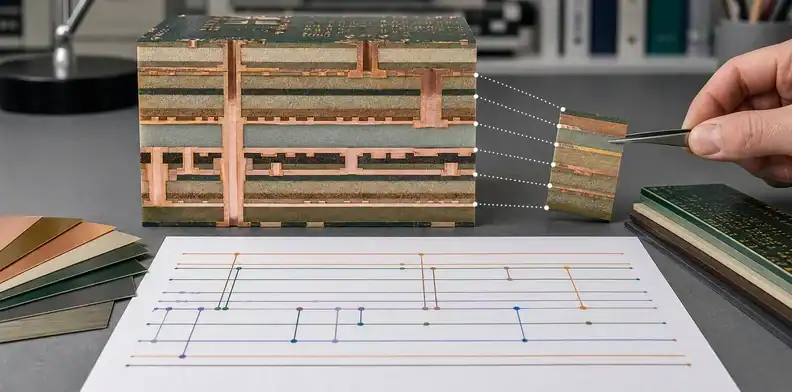
The via method should follow the dielectric it enters and the connection it must make. A laser microvia in a thin build-up dielectric is not the same process as a mechanically drilled blind hole through a thicker subassembly. A buried core via may be drilled and plated while its target layers are still accessible, then enclosed during a later lamination.
Hybrid construction adds a question: does the via stay within an FR4-like subassembly, stay within the low-loss material, or cross the boundary between them? PTFE-based surfaces may need different activation from epoxy. Material movement during lamination can also change landing margin. A supplier who can make conventional 1+N+1 HDI is not automatically confirming every PTFE/FR4 via route.
Ask the fabricator to identify which vias are laser drilled, which are mechanically drilled, which are plated before final lamination, and which see the final through-hole process. The buyer does not need a confidential recipe, but the returned stackup should make the production sequence understandable.
Isola’s public work on hybrid automotive radar construction notes that some material combinations introduce plasma etch, plasma desmear, or multiple surface-treatment steps. That is a useful warning against assuming that a familiar HDI diagram has the same processing cost in every laminate system.
Interface signal: Keep a via within one compatible dielectric group when the electrical design allows it; crossing material families should be an explicit DFM decision.
Count lamination cycles instead of counting labels
Cost and schedule are driven by the number and order of manufacturing stages, not by how many times the word “blind” appears in the legend. A single pair of outer microvias may fit a straightforward build-up route. Several overlapping buried spans can require subassemblies, drilling and plating between presses, and additional registration control.
Ask the supplier to return a simplified build sequence with each sub-lamination, drill, metallization, fill, and final lamination stage. This makes quote comparisons more meaningful. One supplier may reconfigure layer spans to reduce cycles; another may price the released structure without proposing a simpler route.
The cycle map should also identify when critical low-loss material is introduced. Repeated thermal and pressure exposure must be compatible with that laminate and bonding system. The decision belongs in the joint DFM review, not in an after-order CAM message.
| Construction pattern | Typical reason | Quote question |
|---|---|---|
| Outer microvias only | Fine-pitch escape on top and bottom | Can both sides use one build-up sequence? |
| Buried core via plus outer microvias | Dense BGA escape with internal routing | How many subassembly and press stages are needed? |
| Stacked microvias | Very tight routing or vertical interconnect | What fill, cap, and thermal evidence applies? |
| Mixed mechanical and laser vias | Thickness and density vary by span | Which features set the registration window? |
Cost check: Compare the manufacturing sequence, not a single unit-price premium for “HDI.” The sequence explains why two apparently similar quotes differ.
Compare blind, buried, through, and backdrilled paths
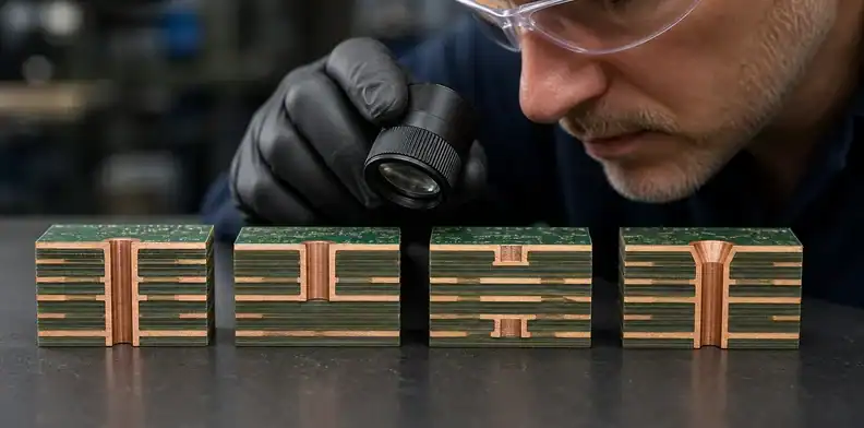
Not every unwanted stub or routing blockage requires a blind via. A plated through-hole may be cheaper and easier to inspect. Backdrilling can remove part of a high-speed stub without creating the same sub-lamination route. Layer reassignment or a different BGA escape pattern may reduce via complexity before fabrication.
The trade-off should be made by function. For a dense component, blind microvias may create routing channels that a through-hole consumes. For a high-speed transition, a through-hole plus backdrill may meet the electrical target with fewer press cycles. For an RF layer near the surface, an edge or surface launch may avoid crossing the full hybrid stack.
Use the PCB backdrill requirements article when the alternative is stub removal. Use HDI microvia aspect ratio when laser via geometry controls the decision. The hybrid RFQ should point to the selected route rather than mixing all options in one ambiguous note.
Decision owners also differ. Signal-integrity engineering decides whether the electrical alternative works. PCB design decides whether routing and pads fit. The fabricator confirms the process window. Purchasing compares the added cycles and evidence. A good DFM record keeps those approvals separate.
Decision point: Use the least complex via route that still meets escape, stub, current, and RF performance requirements for the released design.
Define fill, cap, and land requirements clearly
Via fill and cap instructions affect both fabrication and assembly. A via-in-pad under a BGA may need fill and planarization so solder does not drain into the hole. A buried via may be filled for mechanical or lamination reasons. A blind via that is merely covered by solder mask is not equivalent to a copper-filled and capped microvia.
State the required finished condition instead of using “plugged,” “filled,” and “capped” interchangeably. Identify whether the via receives component soldering, whether another via is stacked on it, whether the surface must be planar, and which side is exposed. The via tenting, plugging, and filling comparison gives the terminology boundary for the purchase note.
Land geometry needs the same care. The fabricator may request larger target lands, a staggered structure, a different dielectric thickness, or a changed laser diameter to improve manufacturability. Those changes can affect routing density or impedance reference geometry, so the RFQ should name who may approve them.
A high-density drawing should also distinguish design nominal from finished requirement. Plating, etch compensation, and planarization change the manufactured feature. Engineering should review the returned CAM proposal against the pad stack and component escape, not only against the original drill file.
Feature rule: Describe the finished via surface and connection function; do not let an undefined process word decide the assembly result.
Ask for evidence that represents the hidden structure
Buried features cannot be judged by final visual inspection. The evidence plan should be agreed while coupon space, section locations, and test structures can still be included in the panel. Electrical test checks connectivity, but it does not show fill quality, landing condition, copper continuity through a stack, or registration at a buried interface.
Microsection evidence should represent the difficult via group. X-ray may help evaluate alignment or filled structures, depending on feature and equipment, while destructive cross-section gives a local view of the actual construction. Thermal evidence may be requested when stacked structures, new material combinations, or end-customer requirements make latent failure a material risk.
| Evidence | Best question answered | RFQ detail needed |
|---|---|---|
| Electrical test | Are required nets connected and isolated? | Test method and netlist revision |
| X-ray image | Is the hidden structure aligned or filled as expected? | Via group, view, and disposition rule |
| Microsection | Are lands, copper, dielectric, and fill built correctly? | Coupon/location and measurements |
| Thermal reliability result | Does the representative structure remain stable? | Method, cycles/exposure, and pass criterion |
The PCB microsection report requirements page helps define traceable report content. For complex microvia structures, connect the plan to HDI thermal cycling qualification rather than claiming that one room-temperature image proves service life.
Evidence call: Match each report to a specific hidden feature and acceptance question; generic inspection certificates do not close a hybrid HDI risk.

Release a buildable hybrid HDI package
Send one controlled package containing fabrication data, the layer stack, via-span table, drill files, fill and cap notes, finished board thickness, controlled impedance requirements, material callouts, quantity, acceptance class, assembly profile, and requested evidence. Include the 3D model or critical mechanical drawing when connector or enclosure fit depends on board thickness.
Ask the supplier to return four items before release: the proposed build sequence, all geometry changes, the evidence plan, and the commercial effects of the chosen route. If a supplier proposes merging via spans or changing stacked to staggered structures, engineering should approve the routing and signal effect before purchasing accepts the revised price.
Keep the response with the hybrid PCB stackup drawing and the supplier’s processed-data approval. That record becomes the baseline for the first lot and repeat orders. It also prevents a later buyer from treating the structure as a generic HDI board after special hybrid processing was used.
A clear RFQ note can say: “Quote the attached hybrid PCB with the layer spans listed in the via table. Return the proposed sub-lamination and drilling sequence, identify each laser and mechanical via, confirm fill and cap assumptions, and quote the named X-ray, microsection, electrical, and thermal evidence. Hold for approval before changing any via span, material boundary, or stacked relationship.”
That instruction invites the fabricator to improve the route while preserving the buyer’s approval boundary. It also gives purchasing a comparable scope across bidders.
FAQ
Are blind vias always laser drilled?
No. Blind holes may be laser drilled or mechanically formed depending on diameter, depth, dielectric, aspect relationship, and supplier process. The RFQ should define the layer span and finished requirement, then ask the fabricator to confirm the method.
Do buried vias always require an extra lamination cycle?
Often they require a subassembly that is drilled and plated before being enclosed, but the total cycle count depends on the complete stack and other via spans. Ask for the actual build sequence rather than assuming one fixed premium.
Can a blind via cross from PTFE into FR4?
It may be feasible, but it creates a mixed-material drilling, preparation, landing, and registration question. Treat that span as a DFM item and require the supplier to confirm the route for the exact materials.
What files help a supplier quote hybrid HDI correctly?
Send fabrication data, a controlled stackup, via-span table, drill files, fill and cap requirements, finished thickness, impedance notes, quantities, assembly exposure, and required inspection reports. A labeled layer map prevents many early quote assumptions.
Review a mixed-material HDI RFQ with QueenEMS
If your PCB or PCBA project combines low-loss material, FR4, and blind or buried vias, send QueenEMS the stackup, via-span table, Gerber or ODB++ files, drill data, component constraints, quantities, and required evidence through the contact page. We can review the intended build sequence, identify open material-interface questions, and prepare a quotation with the via assumptions and inspection scope stated clearly.
Sources
Written by the QueenEMS Engineering Team
Upload your files today · Free DFM check before production · Ship worldwide
Get your PCB prototypes in as fast as 24 hours. We handle FR4, Rogers, and hybrid boards up to 40 layers in volume production, with advanced builds subject to engineering review — free prototypes for 2–4 layer FR-4 boards, no minimum order.
Just upload your Gerber + BOM — we source every part, assemble, and inspect (AOI + X‑Ray) so you don't have to chase suppliers. Boards ship in as fast as 24 hours.