
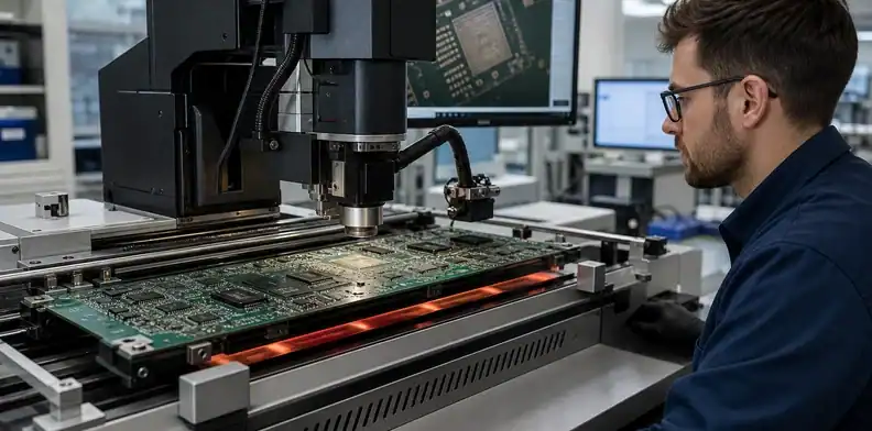
Quick Answer: Large PCB rework should start with defect confirmation, repair authority and a measured thermal plan—not a hotter nozzle. Support the complete assembly, use bottom heat to reduce the local thermal demand, monitor risk locations, limit attempts and verify the repaired joint, surrounding laminate, board shape and function before release.
Large PCB rework becomes difficult because copper planes, heavy components and broad laminate spans redistribute heat and mechanical load. A solder joint may remain solid while the package surface overheats; an edge-clamped board may sag during preheat; repeated attempts may consume pad adhesion before the technician knows the original defect was misdiagnosed.
Before repairing an oversized assembly, establish whether the affected unit can be heated, supported and inspected without creating further damage. The large PCB design recommendations address prevention, and the PCBA rework-causes discussion helps trace upstream defects. The repair decision still needs a method and acceptance evidence for the identified unit.
Table of Contents
- Authorize the repair before applying heat
- Fit the board, heater and support system
- Build a measured large PCB rework profile
- Remove the component without consuming the board
- Prepare pads and place the replacement
- Inspect the repair beyond visible joints
- Close traceability and lot risk
- Quote a controlled large-board repair
Authorize the repair before applying heat
The repair traveler should identify product part/revision, serial or lot, defect location, evidence, component, required result and authorized process. Confirm that the symptom belongs to the component or joint being targeted. A functional failure can originate in firmware, an upstream rail, a cracked via, a connector or an adjacent device; heating the most suspicious package may erase evidence without fixing the cause.
Confirm the defect and repair objective
Review AOI/X-ray, electrical measurements, test logs and visual evidence. Define whether the task is removal for failure analysis, replacement with a new component, reball and reinstall, pad repair, connector replacement or solder-joint correction. Each has different tooling and post-repair proof.
Record the component manufacturer part number, moisture sensitivity/handling state where relevant, solder alloy, underfill or adhesive, thermal-pad connection, neighboring temperature limits and any customer restrictions. Check whether coating, staking, heatsinks or mechanical hardware must be removed under a separate approved instruction.
Set stop rules before work begins
Define maximum heat cycles or attempts, pad/land damage criteria, allowable board discoloration or deformation, adjacent-component protection, rework skill qualification and who can authorize a deviation. State when the assembly becomes scrap, engineering evaluation or failure-analysis material.
A “try again until it works” approach hides cumulative damage. Count prior repair history on the same site and nearby thermally affected area. If the record is incomplete, treat that uncertainty as risk rather than assuming a virgin board.
Decision point: No heat is applied until the defect basis, intended component/site, allowed process, attempt limit and required verification are recorded.
Fit the board, heater and support system
Rework-system capacity is three-dimensional and thermal. Ersa publishes an HR 600 XL work range for assemblies up to 625 x 625 mm with a matrix bottom-heating concept. This equipment example is neither a universal maximum nor proof of a specific factory’s service capacity. Confirm the proposed preheater’s active heating area and thermocouple connections for the actual board.
| Capacity check | Why it matters | Required confirmation |
|---|---|---|
| Complete board and hardware outline | Product must load without collision | Usable work envelope and access |
| Heater coverage relative to repair site | Controls thermal gradient and local demand | Board/site position over heater |
| Top-tool/nozzle clearance | Tall parts can block vertical travel | 3D component map or dry run |
| Support contact and adjustment | Hot board can sag or shift | Tooling drawing and loaded trial |
| Bottom-side component clearance | Heater/support may contact parts | Underside height/keepout map |
| Extraction, optics and pickup | Removal needs visibility and stable lift | Full motion rehearsal |
Support the board near the repair zone and across long spans while preserving bottom heat and bottom-component clearance. Edge clamps alone may define position but not control mid-span movement. Avoid contact beneath fragile packages, exposed solder joints or areas that expand against rigid pins.
Perform a cold dry run with the actual nozzle, pickup, optics and replacement component. Verify that the tool can approach, lift and leave without crossing a tall neighbor. Define how the board is loaded and removed without flexing after a hot cycle.
The chosen preheater does not need to warm every square millimeter equally, but its relationship to the repair site and surrounding mass must be characterized. If the board must be repositioned during one repair, the profile requires revalidation.
Build a measured large PCB rework profile
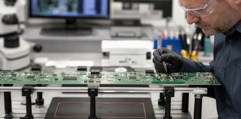
Forum posts about solder refusing to melt often describe large ground planes conducting heat away faster than a hand tool supplies it. Raising tip or hot-air temperature can increase the gradient and damage risk without proving joint temperature. A controlled profile uses broad preheat to reduce local demand and targeted heat to reach reflow under monitored limits.
Place thermocouples at risk locations
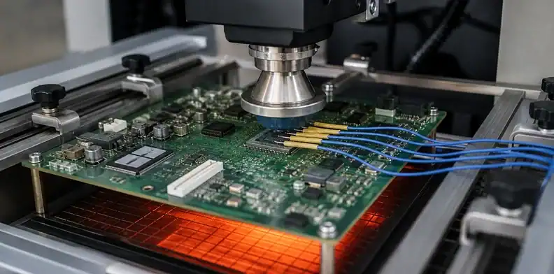
Use a representative populated assembly or approved profile vehicle. Measure near the target joint/package, on the opposite board side, at a sensitive adjacent component, and at a location representing the high-copper heat sink or cold region. Add channels for known component-body limits where required.
Document thermocouple attachment, exact location photographs, logger/channel, sample rate and acceptance source. A wire lying on solder mask reports air or surface contact inconsistently; attachment quality is part of the evidence. Treat a sudden temperature drop during continuous preheating as a possible sensor fault before adding more heat. Check thermocouple attachment and the other channels, and stop the cycle when the control measurement is no longer trustworthy. HAKKO describes this type of anomaly detection on its FR-870B and FR-872 preheaters; confirm the behavior of the actual rework system rather than assuming it has the same interlock. Record the interrupted cycle in the unit’s heat history before deciding whether another attempt is allowed.
Balance bottom and local heat
Develop preheat, soak, local reflow and controlled cooling around the solder alloy, component and board limits. Bottom heat should raise the assembly region without causing widespread unintended reflow or exceeding neighboring restrictions. The top heater then supplies the remaining localized energy.
IPC technical material on large-area-array rework discusses high-thermal-mass assemblies and controlled preheat/reflow. Use such references to understand the process, but derive actual limits from the approved component, solder, board and customer requirements. The large PCB thermal-profile guide provides a disciplined way to select representative hot/cold measurement points.
Run the profile without component removal first when risk justifies it. Review gradients, time above relevant temperatures, peak, cooling and board shape. Lock heater settings, nozzle, board position, support and program as one revision.
Remove the component without consuming the board
Preparation should expose the joint while shielding parts that cannot tolerate the planned airflow or radiant heat. Remove heatsinks, hardware, coating, staking or underfill only through approved methods. Protect nearby plastics and small components without reflecting heat unpredictably onto the target.
Protect adjacent features
Map the thermal and mechanical keepout. Select a nozzle that covers the package/joint region without blasting neighboring components. Confirm that shielding does not obstruct temperature measurement or trap excessive heat. Secure loose cables and hardware outside the airflow.
Apply the approved flux in a controlled amount. Excess flux can boil, contaminate optics, move adjacent chips or hide the moment of reflow. Underfill, corner bond or adhesive changes the removal method and may make ordinary lifting unacceptable.
Lift only after complete reflow
Use the programmed profile and observe the approved reflow indicator. The pickup should lift vertically with minimal force only after all connections are molten. Twisting or prying against partially solid joints tears pads and can distort the package.
Record actual temperature trace and any abnormal event. If the component does not release within the qualified window, stop and diagnose heater contact, thermocouple attachment, solder condition, underfill and thermal path. Do not simply extend dwell beyond the authorization.
After removal, allow controlled cooling if the next operation cannot begin within the approved hot-state window. Inspect the site before cleaning away every clue: lifted pad, mask blister, pad contamination or uneven solder may explain the failure and affect repair viability.
Removal rule: Mechanical lift force must never substitute for complete, measured solder reflow.
Prepare pads and place the replacement
Evaluate land integrity, solder mask, exposed dielectric, vias and local board flatness under magnification. Compare the site with the design data and an approved reference. If pads are lifted, barrels damaged or laminate delaminated, stop for engineering disposition rather than hiding the condition beneath a new component.
Remove residual solder with a controlled method matched to pad size and thermal mass. The general solder-wick rework guide explains wick technique; on a large board, preheat and tool capacity still govern whether the pad is cleaned without prolonged contact. Avoid scraping mask or copper.
Clean the site with approved chemistry and verify residue removal/dryness. Inspect pad coplanarity and condition again. Record any pad repair separately with its approved method and inspection.
Prepare the replacement component according to moisture, solderability, ball/lead condition and handling requirements. Use controlled paste, flux, preform or reballed component as specified. Align through optics or a validated placement method; package outline alone may not guarantee ball-to-pad registration.
Run the qualified replacement profile. The attachment cycle can differ from removal because a new component, flux and solder volume respond differently. Record component lot/date code where required and preserve the trace.
Cool the assembly in support before moving it. Early lifting or fixture release can shift molten joints or bend the hot board. Remove temporary protection and perform a preliminary visual/site check before advanced inspection.
Inspect the repair beyond visible joints
Verification should match the joint geometry and original failure. Visible leaded joints may support optical inspection; bottom-terminated packages often need X-ray; a functional symptom may require electrical, programming or system test. One green check does not replace the full repair objective.
Match evidence to joint geometry
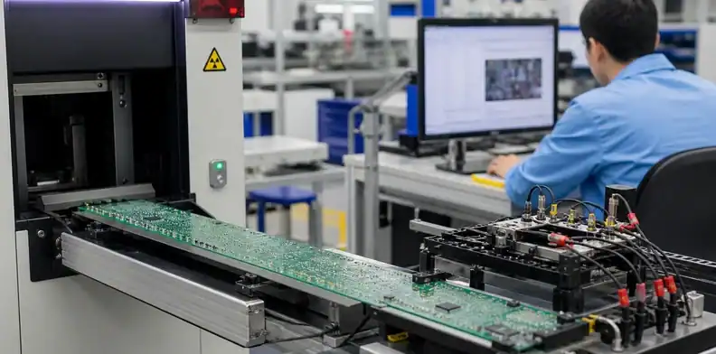
For BGA, LGA or thermal-pad packages, use the approved X-ray inspection framework to evaluate features accessible to radiography, while acknowledging method limits. For connectors, inspect seating, barrel/joint condition and mechanical datum. For fine-pitch leads, check alignment, wetting, bridges and lifted leads.
Compare repaired and nearby unaffected areas when useful. Inspect for shifted small components, solder balls, mask damage, delamination, scorching, disturbed coating or hardware damage created by the heat/airflow.
Recheck board shape and function
Measure free-state or supported board shape at a defined condition if the repair zone or heating span could cause distortion. Verify critical connector fit and mounting interfaces after the board returns to ambient temperature. A local electrical pass cannot close a new mechanical problem.
Repeat the test that exposed the original defect, then run any required regression test for adjacent functions and power rails. Define firmware, fixtures, limits and result logs. If the failure was intermittent, use an approved stress or repeat sequence rather than one power-on.
Inspection findings should link to the actual rework profile and technician. A repaired unit that fails again returns to the stop rule; it does not automatically receive another uncontrolled cycle.
Evidence check: Release the repair only when joint-specific inspection, board condition and the test that exposed the original failure all support the disposition.

Close traceability and lot risk
The final traveler should include product serial/lot, failure evidence, component identity and lot, repair site, prior history, equipment/tooling/program, thermocouple map and profile, removal/site findings, replacement process, inspection, test, board-shape check, deviations and disposition. Photos need scale and location, not anonymous close-ups.
Decide whether the defect is isolated or indicates lot/process risk. A cracked component from handling may require containment of similar boards. Insufficient solder across one package type may require stencil/profile/AOI review. Use the PCBA defect Pareto method to connect individual repairs to recurring causes rather than celebrating repair yield.
Record as-built configuration after repair. If a substitute component, jumper, pad repair or coating restoration exists, receiving and future service teams need that controlled information. Apply customer deviation approval where required.
Change triggers include a new board revision, laminate/copper distribution, component package or supplier, solder alloy, preheater, nozzle, support, thermocouple method, profile or inspection method. Assess whether previous qualification still represents the repair.
Retain removed components for failure analysis when instructed, with identification and ESD/moisture protection. Do not mix failed parts or lose orientation evidence. The cost of a component is often smaller than the information it contains about a systemic issue.
| Traceability item | Required link | Risk it controls |
|---|---|---|
| Failure and site evidence | Serial, reference designator and diagnosis | Repairing the wrong cause |
| Thermal and tooling record | Profile, support, nozzle and operator | Unrepeatable or excessive heat |
| Replacement and verification | Component lot, inspection and test | Hidden configuration or escape |
Record rule: A repaired board cannot return to the lot until its component, heat history, inspection and final disposition are linked to the unit.
Quote a controlled large-board repair
Provide product drawing/data, assembled dimensions, mass, height map, board stack-up/copper information, BOM and target component, failure evidence, solder alloy, coating/underfill/staking, prior rework history, neighboring restrictions, acceptance criteria, required inspection/test and allowed disposition. Supply a sample or representative spare when profile development requires one.
Ask the repair source to state:
- rework-system envelope, heater coverage and board position;
- support and underside-clearance plan;
- nozzle/pickup/optics access and shielding;
- profile development method and thermocouple locations;
- removal, pad-preparation and replacement materials;
- maximum attempts and stop criteria;
- X-ray/optical/electrical/mechanical evidence;
- serialization, removed-part handling and report format.
Price diagnosis, profile/tooling development, repair, inspection and test separately. A supplier cannot responsibly quote a guaranteed fix when the defect mechanism and land condition remain unknown. Define evaluation-only and no-repair outcomes.
Use the large PCB handling guide to define transport and support before and after hot work. Protecting the unit outside the rework station is part of the repair route.
Quotation request: Start the repair-feasibility review on the QueenEMS Large Format PCB page with board dimensions, component/site data, copper context, failure evidence, prior heat history and required verification. Require the response to define support and measured thermal control before any component is lifted.
FAQ
Why will solder not melt on a large PCB?
Large copper areas, planes, heat sinks and components can conduct energy away from the joint. The solution is not automatically a higher setpoint; use adequate tool power, broad preheat and measured joint/board temperatures.
Must the whole large board be preheated?
The qualified heating area must reduce local thermal demand without creating harmful gradients elsewhere. The required coverage depends on repair location, board construction, components, support and equipment.
How many times can one component site be reworked?
There is no safe universal count. The product/quality plan should set limits based on materials, prior history, observed site condition and customer requirements, with a stop-and-disposition rule.
Can functional test replace X-ray after BGA rework?
Functional test and X-ray answer different questions. Functional success does not directly reveal every concealed-joint condition, while X-ray does not prove every function. Use a risk-based combination.
What makes a large-board repair report useful?
It connects the identified unit and site to failure evidence, equipment/profile, actual temperature trace, component lot, site findings, replacement, inspection/test and final authorization.
Sources
Written by the QueenEMS Engineering Team
Upload your files today · Free DFM check before production · Ship worldwide
Get your PCB prototypes in as fast as 24 hours. We handle FR4, Rogers, and hybrid boards up to 40 layers in volume production, with advanced builds subject to engineering review — free prototypes for 2–4 layer FR-4 boards, no minimum order.
Just upload your Gerber + BOM — we source every part, assemble, and inspect (AOI + X‑Ray) so you don't have to chase suppliers. Boards ship in as fast as 24 hours.