

Quick Answer: BT substrate warpage is mainly driven by thin construction, CTE mismatch, asymmetric copper, resin shrinkage, die attach stress, and reflow heating. Control starts with symmetric stack design, low-CTE material selection, copper balance, cure-profile discipline, and warpage measurement before assembly release.
Key takeaways
- Warpage is not only a factory defect; it can be designed into the stack before fabrication starts.
- Thin BT carriers, large die, unbalanced copper, and aggressive reflow profiles raise coplanarity risk.
- Low-CTE BT grades and symmetric layup help, but they must be matched with process control and measurement.
- A quote should state the warpage target, measurement condition, assembly temperature, and evidence expected before shipment.
Warpage turns a good substrate drawing into an assembly problem. BGA balls may not wet evenly, wire-bond pads may shift, lids may not seal, and a thin module may fail height inspection. This article focuses on BT and thin package substrates, not generic board bow and twist. The related BT substrate guide ties this detail back to BT material behavior, package substrate choices, and buying checks.
| Warpage driver | Why it matters | Control lever |
|---|---|---|
| Thin BT carrier | Low stiffness | Thickness and support review |
| CTE mismatch | Bending during heat | Low-CTE material and die data |
| Asymmetric copper | Built-in stress | Stack symmetry and copper balance |
| Measurement condition | What it proves | When to request |
|---|---|---|
| Room-temperature unit | Basic flatness | Incoming inspection |
| After simulated reflow | Assembly stability | Fine-pitch packages |
| Panel or strip check | Process drift | Repeat production lots |
Table of Contents
- Why do BT substrates warp?
- How CTE mismatch drives warpage
- Design fixes: symmetric stackup and copper balance
- Material fixes: low-CTE BT and fillers
- Process fixes: cure profile control
- What warpage spec should you target?
- How warpage is measured before assembly
- What to send for a warpage review
Why do BT substrates warp?
BT substrates warp when stresses through the stack are not balanced. Thin organic material, copper distribution, die attach, resin shrinkage, glass reinforcement, and reflow heating all contribute. A thick ordinary PCB may hide some imbalance; a thin BT package carrier usually cannot. Root-cause signal: Warpage is a stack and assembly interaction, not a single material property.
How CTE mismatch drives warpage
CTE mismatch drives warpage because silicon, copper, resin, glass, solder, mold compound, and any lid or stiffener expand differently. During heat-up and cool-down, those materials pull against each other. For memory and low-CTE package context, see low-CTE BT for memory. CTE rule: Match the BT stack to the die and assembly temperature, not only to a room-temperature datasheet.
Design fixes: symmetric stackup and copper balance
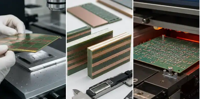
Symmetric stackup is the first design fix because it balances resin, glass, and copper around the neutral axis. Copper balance is the second fix because local copper density can pull the substrate during lamination and reflow. Copper balancing must respect electrical and RF requirements. Design rule: A flat BT substrate starts with balanced geometry before the supplier touches the press.
Material fixes: low-CTE BT and fillers
Low-CTE BT grades and filler systems help reduce movement and shrinkage. MGC describes low-CTE and low-shrinkage BT families for IC package use, including options suitable for coreless process. A generic BT substitute may not provide the same low-CTE behavior. Material call: Low-CTE BT is a warpage tool, but it must stay compatible with via, RF, and assembly requirements.
Process fixes: cure profile control
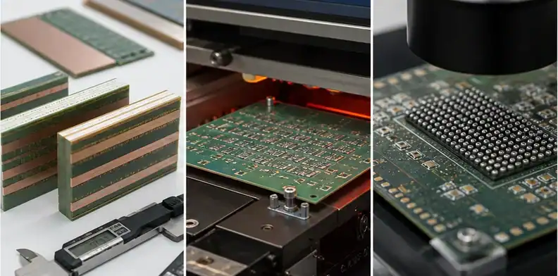
Cure profile control affects residual stress, resin flow, voids, and flatness. A supplier’s lamination recipe determines how the stack heats, flows, cures, and cools. The BT lamination and cure control article explains this stage in detail. Process rule: Warpage control continues through assembly; fabrication flatness alone is not the final proof.
What warpage spec should you target?
A common practical target for many SMT-related boards is around 0.5% of diagonal or tighter when package coplanarity demands it, while broader board requirements may allow more. For BT package substrates, the correct number should come from ball pitch, module height, and customer acceptance. Spec rule: A BT warpage target must say what is measured, when it is measured, and which assembly risk it protects.
How warpage is measured before assembly
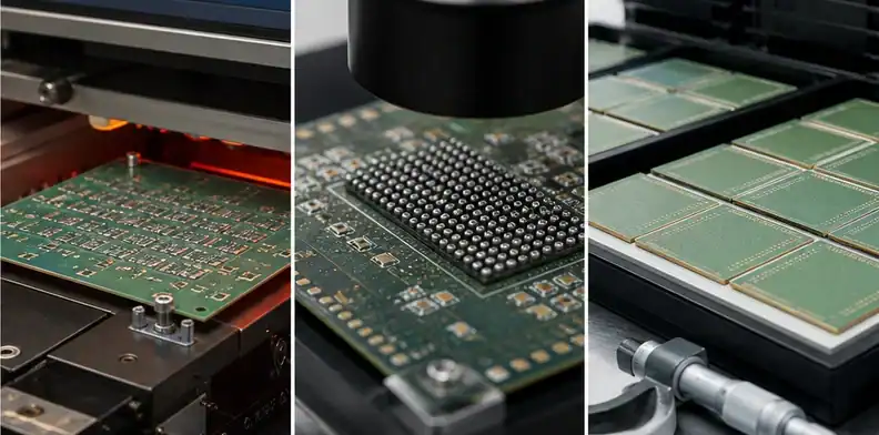
Warpage can be measured with flatness inspection, optical profiling, shadow moire, laser scanning, thickness mapping, or fixture-based methods depending on substrate type and customer need. Ask whether measurement is performed on the panel, singulated substrate, after bake, after simulated reflow, or at room condition only. Measurement signal: Warpage evidence is useful only when the method and condition are stated.
What to send for a warpage review
Send stack-up, Gerber or ODB++ files, copper density, finished thickness, material target, die or component size, assembly reflow profile, ball pitch or pad geometry, and required flatness condition. For assembly implications, the QueenEMS BGA assembly reliability page gives useful context. Keep the flatness requirement with the stack, die, and reflow assumptions so receiving and assembly judge the same condition that the supplier quoted.
Extra buyer notes for assembly handoff
Warpage should be reviewed at the handoff between fabrication and assembly. A substrate may pass outgoing inspection at room temperature but deform during preheat, peak reflow, or cooling. If the assembly process has fine-pitch BGA, large die attach, or tight module height, the buyer should ask whether room-temperature flatness is enough evidence.
Fixture and carrier choices can hide or create warpage issues. A carrier may hold a thin BT substrate flat during placement, while the part still bends after release. That may be acceptable if the final package is constrained, or unacceptable if the finished module must stay flat by itself. The assembly owner should define which condition matters.
Measurement sampling should match risk. A first article may need more measurements than a repeat production lot, especially when the stack is new or the die size has changed. Once the process is stable, the inspection plan can be adjusted, but the acceptance limit should remain tied to the assembly need.
A useful supplier reply separates design fixes, material fixes, and process fixes. Symmetry and copper balance belong to design review. Low-CTE BT belongs to material selection. Cure and cooling belong to fabrication control. Reflow support and carriers belong to assembly. Clear ownership prevents the same warpage problem from being passed between teams.
The buyer should state whether the warpage concern is bare-substrate assembly, die attach, wire bonding, solder-ball attach, or final module installation. Each stage has a different tolerance window. A substrate that is flat enough for SMT may still be marginal for a fine wire-bond process or a tight optical module.
Panel versus unit measurement can also change the result. A panel may look acceptable while individual units warp after singulation, or a singulated unit may relax after being removed from the panel. Ask which condition the supplier measures and which condition the assembler needs.
Thermal history should be recorded. Baking, lamination, finish processing, storage, and reflow can all change stress state. If a lot is reworked or exposed to an extra thermal cycle, the warpage evidence from the original condition may no longer describe the parts going into assembly.
Warpage review should include the attached die or component whenever possible. Bare BT flatness is only the starting point. A large die, uneven mold compound, or local stiffener can change the final bow. If the supplier only fabricates the bare substrate, the assembly owner should complete the package-level flatness review.
For repeat production, define a practical hold point. If measured warpage exceeds the limit, the lot should not move directly into assembly while teams debate responsibility. The record should say who reviews the deviation, what evidence is needed, and whether the lot can be used for prototype learning or must be rebuilt.
Warpage risk review by package type
A fine-pitch BGA substrate has little tolerance for bow because ball contact depends on coplanarity. The buyer should connect the warpage limit to ball pitch and assembly profile. If the design uses a thin BT carrier and small solder balls, room-temperature flatness may not be enough; hot warpage may matter more.
A wire-bond package has a different sensitivity. Excessive bow can change bond tool contact, loop height, or pad position. The supplier may deliver a substrate that is electrically correct but difficult to bond repeatably. In that case, the flatness requirement should be tied to bonding, not only to soldering.
A sensor module may care about package alignment or calibrated spacing. Warpage can shift a lid, port, optical path, or die position. The substrate supplier may not own sensor calibration, but it should understand which flatness feature protects the module.
Large die attach creates another risk pattern. A silicon die can stiffen one side of the BT carrier and add stress during cure and reflow. The buyer should provide die size and placement during substrate review so the supplier can judge copper balance and material CTE with the real assembly in mind.
For repeat production, warpage data should be trended enough to catch drift. A lot may pass the limit, but a gradual move toward the edge of the window can predict future assembly trouble. Overseas buyers should ask for concise evidence that can be read by both engineering and receiving teams.
Practical release limits for warpage-sensitive BT
A practical warpage limit should be linked to what fails. For fine-pitch soldering, the limit protects ball contact and joint formation. For wire bonding, it protects tool contact and loop stability. For sensor modules, it protects alignment, height, and package stress. Without that link, the number becomes a generic tolerance.
The buyer should ask whether the supplier’s measurement is performed before or after any bake, simulated reflow, or singulation. A substrate may change shape after these steps. The measured condition should match the condition that the assembler cares about.
Design changes should be considered before process fixes. If the stack is extremely asymmetric, no cure profile can fully remove the stress. Copper balance, thickness change, or material change may be needed before the supplier can commit to flatness.
Assembly teams should also avoid creating warpage after a good substrate is delivered. Uneven heating, poor support, aggressive reflow, or unsuitable carriers can bend thin BT. The substrate supplier and assembler need a shared view of the thermal path.
When a lot is near the limit, decide whether it is usable for prototype learning, pilot build, or production shipment. Mixing these decisions causes confusion. A clear release category lets the team learn from marginal parts without accidentally approving them for customer production.
How to read a warpage supplier response
A good supplier response should name the suspected driver. It may be copper imbalance, thin construction, low-CTE material need, die attach stress, or assembly support. A vague statement that warpage will be controlled does not tell the buyer what risk remains.
The response should also say whether the risk is design-driven or process-driven. Design-driven issues need stack, copper, thickness, or material changes. Process-driven issues may be addressed with lamination, cure, cooling, handling, or fixture control. Mixing these categories creates slow corrective action.
For a first article, ask for enough evidence to decide whether the design can move forward. That may be a measured warpage value, a photo under fixture, a profiling report, or a note that the lot was measured after simulated reflow. The evidence should match the actual assembly concern.
For repeat production, ask what the supplier will monitor. Warpage is easier to manage when the process watches the trend instead of reacting only when assembly fails.
A final warpage review should include packaging and shipment. Thin BT substrates can be damaged or stressed by poor stacking, trays, vacuum packs, or handling after inspection. If the substrate is measured flat at the factory but arrives bent, the team loses time arguing about when the problem occurred. Ask the supplier how sensitive substrates are packed and whether receiving should inspect flatness before assembly release.
For the first production lot, consider asking the assembler to report whether warpage affected placement, soldering, bonding, or fixture loading. Supplier measurement and assembly feedback together create a stronger baseline than either record alone.
A final buyer habit helps a lot: keep photos or measurement screenshots from the first accepted lot. They give engineering and receiving a practical reference when a later lot looks different. The reference is not a substitute for measurement, but it speeds up triage.
If the project uses several substrate sizes, do not reuse one warpage assumption across all of them. Larger outlines, different copper density, and changed die placement can create a new bending mode even when the material family is unchanged. State whether acceptance applies per unit, per strip, or per production panel, and ask who reviews the deviation if that condition fails. Add this rule before the supplier starts panel planning.
For flatness risk, send the stack-up, copper-density map, die or component size, reflow profile, required condition, and measurement method via the QueenEMS contact page. QueenEMS can test the BT flatness review path against soldering, bonding, receiving inspection, and shipment handling before the lot reaches assembly.
FAQ
Why does BT warp?
BT warps because thin organic stacks amplify CTE mismatch, copper imbalance, resin shrinkage, die attach stress, and reflow heating.
How do you control BT warpage?
Use symmetric layup, copper balance, low-CTE material, controlled cure, appropriate thickness, and measurement under the right condition.
What warpage spec is acceptable?
It depends on package pitch and customer requirement. Many buyers target around 0.5% of diagonal or tighter for sensitive assemblies.
Does thin BT warp more?
Thin BT usually has less stiffness, so the same stress can create more bow or twist than in a thicker carrier.
Sources
- Mitsubishi Gas Chemical, Low-CTE BT resin laminate lineup
- Global Electronics Association, IPC-6921 organic IC substrate standard
Written by the QueenEMS Engineering Team
Upload your files today · Free DFM check before production · Ship worldwide
Get your PCB prototypes in as fast as 24 hours. We handle FR4, Rogers, and Flex up to 60 layers — free prototypes for 2–4 layer boards, no minimum order.
Just upload your Gerber + BOM — we source every part, assemble, and inspect (AOI + X‑Ray) so you don't have to chase suppliers. Boards ship in as fast as 24 hours.