
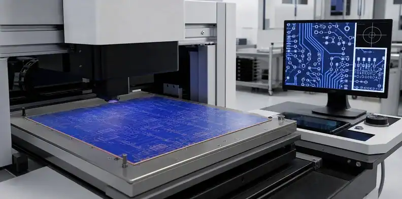
Quick Answer: LDI PCB imaging is acceptable when the developed resist pattern matches the released artwork, remains registered to drilled or laminated targets, and protects the copper through plating or etching. Buyers should freeze the artwork revision, registration references, compensation authority, dry-film process family, critical feature locations, and inspection evidence. LDI improves image placement, but it does not correct dirty copper, unstable resist lamination, uncontrolled development, or incorrect CAM data.
Laser direct imaging (LDI) often appears in supplier capability tables as proof that fine lines are easy. That conclusion skips most of the process. The laser exposes a photoresist image, but final conductor geometry also depends on surface preparation, film lamination, panel movement, exposure, development, plating or etching, and inspection.
For quotation, the important question is not “Do you have LDI?” It is “How will this specific panel be imaged, compensated, inspected, and released?” The answer should connect the design’s critical features to evidence that survives beyond a machine brochure.
Table of Contents
- Map the complete image-transfer chain
- Prepare copper and laminate resist consistently
- Define registration datums and compensation
- Hold exposure and development inside one window
- Use inspection data to separate defect causes
- Treat inner and outer layers differently
- Approve CAM changes without losing design intent
- Build an RFQ package suppliers can compare
Map the complete image-transfer chain
Process rule: LDI controls exposure placement, while copper preparation, film response, development, and later etching still determine the finished conductor.
The finished trace is the result of several linked transformations. CAM prepares the artwork; the panel is cleaned and coated or laminated with resist; the image is registered and exposed; unneeded resist is developed away; copper is plated or etched; resist is stripped; and the conductor is inspected. A weak link anywhere in that chain can create opens, shorts, neck-down, copper residues, pad loss, or registration error.
Start the review with the manufacturing path. Inner layers normally use imaging followed by copper etching. Pattern-plated outer layers use the resist image to define where additional copper and etch resist are deposited before final etching. A defect with the same appearance can therefore have different causes depending on when it formed.
The buyer should identify the features that cannot tolerate ordinary process drift:
- minimum line and space by layer;
- fine-pitch pads and narrow solder-mask relationships;
- capture pads for drilled holes or laser microvias;
- impedance-controlled lines whose finished width matters;
- copper features near routed edges or cavities;
- local areas where dense and open copper patterns meet.
The high-precision line-space RFQ evidence helps establish the finished-feature requirement. The LDI review then determines how the resist image and downstream copper process will preserve it.
Do not use an equipment name as an acceptance criterion. Record the released artwork, finished copper requirement, inspection method and change-control path. Those outputs remain meaningful even if the supplier changes to another qualified imaging platform.
Prepare copper and laminate resist consistently
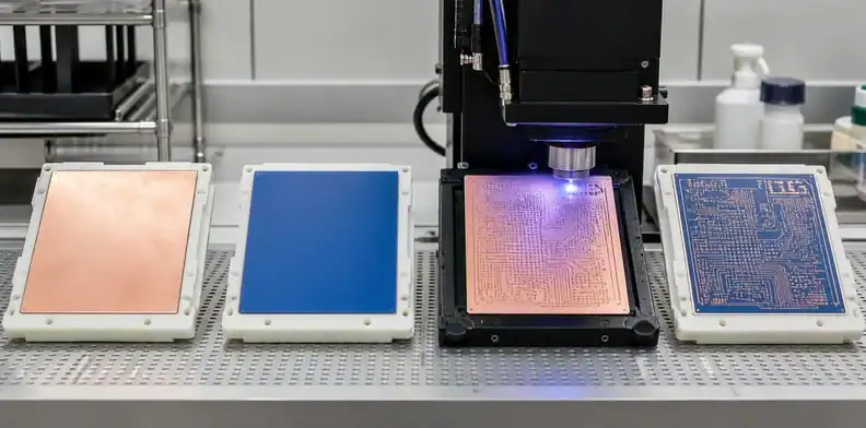
Surface check: Release imaging only after the copper condition and laminated resist meet the qualified handling and inspection window for the selected film.
Photoresist must contact a clean, suitably prepared copper surface without trapped contamination, wrinkles, bubbles or uncontrolled edge lifting. LDI cannot expose a stable pattern through a film that is poorly bonded or unevenly laminated.
Surface preparation has two competing objectives. It must remove oxidation, particles and residues while creating enough surface condition for resist adhesion. It must not remove uncontrolled copper, damage thin foil, or leave chemistry that interferes with lamination. The process window depends on foil type, copper thickness, prior treatment and the resist system.
Dry-film storage and conditioning also matter. A supplier should control shelf life, temperature exposure, handling and time between lamination, exposure and development according to the material process. The buyer rarely needs those proprietary settings, but should ask whether the selected film and process are qualified for the panel thickness, copper topography and required feature size.
For a problem lot, evidence should distinguish an image-data error from an adhesion failure. Useful observations include where lifting began, whether it follows heavy copper steps, whether defects repeat at a panel edge, and whether particles or handling marks are present. A generic “LDI issue” label prevents effective containment because it does not identify the stage that needs correction.
Define registration datums and compensation
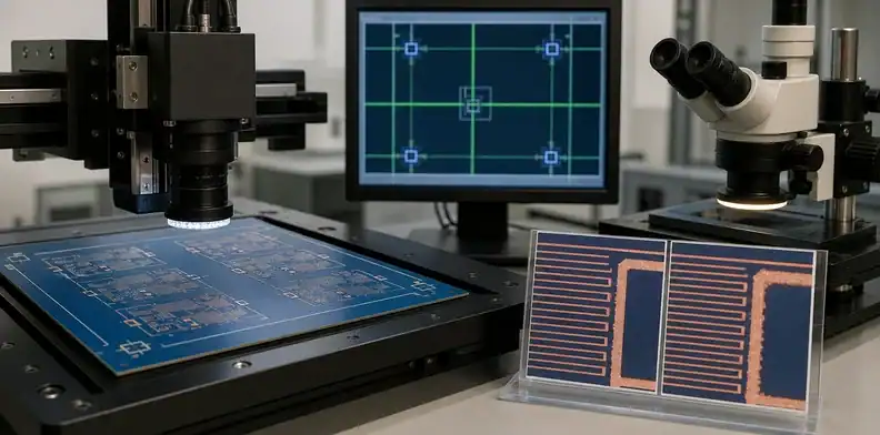
LDI can align an image to panel targets and apply compensation, but the target system must represent the layer that matters. Inner-layer scaling, multilayer lamination movement, drilled-hole position and outer-layer distortion do not collapse into one universal offset.
Define which references control each image:
| Image stage | Useful reference question | Design consequence |
|---|---|---|
| Inner-layer imaging | Is the image tied to tooling targets, panel edges or another controlled datum? | Establishes conductor position before lamination |
| Post-lamination outer imaging | Are buried targets measured optically or by X-ray? | Connects outer pads to internal features |
| Pattern around drilled holes | Does registration use actual drilled locations or nominal CAD coordinates? | Controls annular relationship and breakout risk |
| Fine-line local area | Can global scaling represent local panel distortion? | Determines whether local compensation or panel-size control is needed |
The tolerance budget should include artwork preparation, panel dimensional change, registration measurement, imaging placement, development and conductor formation. The laser’s nominal accuracy is only one term. If an outer pad is barely large enough after all terms are included, the design needs a decision before production, not an optimistic interpretation after inspection.
When drilled features are involved, compare the proposed relationship with the annular ring breakout acceptance. A registration plan should prevent avoidable breakout; it should not be used to normalize a design with no realistic manufacturing margin.
Compensation ownership must be explicit. Routine scale correction within an agreed process window may remain with the supplier. Pad resizing, trace movement, clearance reduction or local artwork distortion should require a marked-up engineering approval because those edits can change electrical and assembly behavior.
Hold exposure and development inside one window
Imaging rule: Exposure and development must be qualified together because changing either operation can move the final resist edge and alter fine-line yield.
The exposed resist image is not the finished resist opening. Exposure energy, focus, resist response, panel surface, development chemistry, spray condition and dwell determine whether the developed wall and opening match the CAM intent.
Underexposure can leave weak resist that lifts or erodes. Overexposure can close narrow spaces or change the developed edge. Incomplete development can leave residue where copper should be removed or plated; aggressive development can attack image edges. The correct response is to control the combined process, not to tune one setting until a single coupon looks acceptable.
Ask how the supplier verifies the image after development and before expensive downstream work. Depending on the layer and risk, this may include automated optical inspection (AOI), test patterns, resist-opening measurements, registration coupons or first-piece review. The evidence should identify both the feature and the artwork revision.
Critical dimensions should be connected to the finished conductor. If a supplier measures only the resist opening but does not account for plating growth or etch behavior, the data cannot predict final line width. For dense outer layers, imaging and copper plating distribution must be reviewed together because deposit thickness affects the geometry that later etching must reproduce.
Use inspection data to separate defect causes
AOI compares the manufactured pattern with the reference data and can identify opens, shorts, nicks, protrusions and other deviations. It does not automatically prove why the deviation occurred. A useful corrective response traces the observed shape back through imaging, development, plating and etching.
Consider four examples:
- A missing copper segment can come from a resist defect before plating, local over-etch, mechanical damage or incorrect source data.
- Copper left between conductors can result from residual resist, under-etch, artwork error or plating that made the etch burden too large.
- A shifted pad field can reflect registration measurement, incorrect compensation, panel movement or the wrong layer revision.
- Repeated edge neck-down can point to dry-film adhesion, spray distribution, panel transport or a design that leaves no process margin.
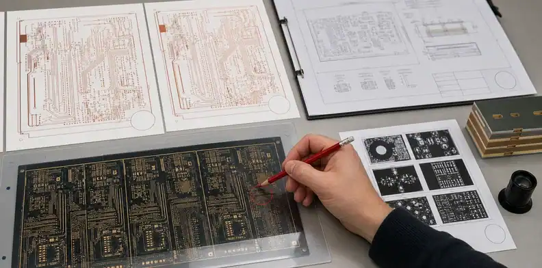
The inspection record should retain defect coordinates, layer, panel position, classification, reference revision and disposition. When repair or CAM modification is proposed, preserve the original evidence and the approved correction. This makes repeat-lot learning possible and prevents a corrected image from erasing the reason for the change.
Inspection sampling should follow risk. A high-density layer with marginal space, a new material construction, a large asymmetric panel or a newly scaled design deserves stronger first-article evidence than a mature, wide-feature layer. The sampling logic should be documented before the supplier finds a defect.
Retain the source and inspection datasets in a form that can be compared. The CAM image used by LDI, the AOI reference, the customer release files and the finished-board netlist should share a traceable revision relationship. Otherwise, an AOI pass may only prove that a panel matches the wrong reference. File manifests, checksums or controlled system records can establish identity without exposing proprietary machine files.
Defect maps are also more useful than isolated photographs. A concentration along one panel edge can indicate lamination or transport effects; repeated locations across panels can point to artwork; random particles suggest handling or cleaning. Ask the supplier to preserve enough coordinate and panel-position data to support that distinction. The buyer can then approve containment based on a mechanism rather than on the number of images in a report.
When an operator overrides an AOI call, the record should retain the original call, classification reason and disposition. False calls are normal in optical inspection, but an undocumented override removes the audit trail needed to understand later opens or shorts.
Treat inner and outer layers differently
Layer call: Use separate registration references and evidence for inner layers, laminated targets, drilled features, and outer-layer images rather than one machine capability statement.
Inner-layer imaging creates copper that will be buried by lamination. Once laminated, direct visual access is gone, so AOI and pre-lamination release controls carry more weight. Outer-layer pattern imaging interacts with drilled holes, copper plating, surface finish, solder mask and final dimensional relationships.
For inner layers, focus on:
- conductor width and spacing after etch;
- residual copper and open-circuit defects;
- registration targets and scaling records;
- cleanliness and handling before oxide or alternative bonding treatment;
- revision identity before lay-up.
For outer layers, add:
- alignment to actual drilled or laser-drilled features;
- resist durability through cleaning and plating;
- plating growth and etch compensation;
- pad and edge geometry used by assembly;
- the relationship to later solder-mask openings.
Do not reuse one acceptance photograph for both stages. The risks, accessible evidence and corrective actions differ. When the outer conductor must support a narrow solder-mask web, coordinate this review with the solder-mask bridge requirements instead of assuming that a correct copper image guarantees a printable mask.

Approve CAM changes without losing design intent
Fine-feature panels often need fabrication compensation. The safe boundary is between process allowance and design change. Scaling an entire layer to account for measured panel movement may be a qualified manufacturing control. Moving a trace, enlarging a pad, reducing a clearance, changing copper density or altering an impedance line is an engineering change.
Every approval request should identify:
- affected layer and coordinate or feature class;
- original and proposed dimensions;
- reason tied to a named process constraint;
- impact on neighboring copper, holes, mask and impedance;
- revised output that will become the build baseline;
- whether the change applies only to a prototype or to repeat production.
Do not approve screenshots without a controlled dataset. After agreement, compare the supplier’s processed Gerber files with the approved mark-up and confirm that only accepted edits were made. The manufacturing package and purchase record should reference the same revision.
An artwork correction discovered after imaging also needs containment. Identify which panels and layers used the wrong data, whether later operations began, and whether the affected material can be reworked without compromising acceptance. Re-exposure or resist stripping is not automatically harmless; the supplier should assess surface condition and process history before reuse.
Build an RFQ package suppliers can compare
The RFQ should expose the imaging difficulty rather than hide it in a generic line-space note. Include the released Gerber or intelligent product data, fabrication drawing, layer stack, copper weights, finished line requirements, controlled-impedance information, drill data, panel constraints and inspection class.
| Imaging input | Required RFQ detail |
|---|---|
| Critical artwork | Layer, revision, minimum finished feature and protected geometry |
| Registration datum | Tooling, target, drilled hole or local alignment relationship |
| Compensation authority | Routine process scaling limit and engineering approval threshold |
| Inspection output | AOI stage, measured feature set, panel location and retained record |
Add an imaging control note that states:
- artwork revision and file manifest;
- critical layers and feature locations;
- minimum finished conductor and spacing, not only nominal CAD values;
- registration relationship to holes, cavities or other layers;
- features that may not be resized or moved without approval;
- first-article measurement and AOI evidence;
- response required when compensation exceeds the agreed window;
- repeat-order record that defines the production baseline.
Compare supplier replies by the chain they control. One may quote finished line width with measured coupons and AOI retention; another may quote only the nominal artwork and a machine capability. Those are not equivalent offers even when the price table looks similar.
For a focused review, send QueenEMS the stack-up, copper weights, critical artwork, minimum finished features, drill relationship, panel requirement and supplier compensation proposal through the QueenEMS contact page. The resulting quotation can then state which dimensions are controlled, what evidence is included and who owns any CAM change.
FAQ
Does LDI eliminate PCB registration errors?
No. LDI can improve image placement and compensation, but total registration still includes artwork, panel movement, target measurement, development and downstream conductor formation.
Is dry-film inspection the same as finished copper inspection?
No. Resist inspection confirms the developed image, while plating and etching can still change final copper width, spacing and edge condition. Use both checkpoints when the feature is critical.
Can a supplier resize pads during LDI compensation?
Only with engineering approval when the resize changes released geometry. Routine process scaling and design edits should have separate authority limits.
What should an LDI first-article report contain?
Require the layer and revision, registration reference, critical feature measurements, AOI result, panel location, compensation record, disposition and the approved baseline for repeat production.
Sources
- IPC, Design for Manufacturing Confirmed by IPC Standards
- IPC, IPC-2581C Generic Requirements table of contents
Written by the QueenEMS Engineering Team
Upload your files today · Free DFM check before production · Ship worldwide
Get your PCB prototypes in as fast as 24 hours. We handle FR4, Rogers, and hybrid boards up to 40 layers in volume production, with advanced builds subject to engineering review — free prototypes for 2–4 layer FR-4 boards, no minimum order.
Just upload your Gerber + BOM — we source every part, assemble, and inspect (AOI + X‑Ray) so you don't have to chase suppliers. Boards ship in as fast as 24 hours.