
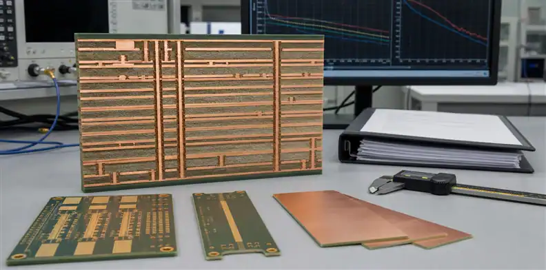
Quick Answer: A Rogers RO1200 PCB material RFQ should identify the laminate and bondply constructions separately, freeze dielectric and copper choices, disclose the channel loss target, and require a returned production stackup plus coupon evidence. RO1200 is positioned for extremely low-loss digital boards, but its published Dk and Df do not guarantee the loss of a finished backplane. Glass style, resin content, copper profile, trace geometry, via fields, press behavior, and the test method still determine whether a supplier’s interpretation matches the model.
Rogers RO1200 PCB material is attractive when a conventional low-loss laminate no longer leaves enough channel margin. The purchasing mistake is to convert that engineering conclusion into a one-line note such as “RO1200 or equivalent.” That wording leaves the supplier to choose the laminate thickness, bondply construction, foil profile, glass style, pressed dielectric thickness, and evidence package.
This article owns the RO1200 quotation and release decision. It does not replace the broader PCB materials guide or the existing Rogers family pages. The goal is a fabrication package that preserves the electrical assumptions behind a high-layer-count design.
Table of Contents
- Confirm that RO1200 solves the actual channel problem
- Distinguish laminate data from bondply behavior
- Normalize Dk and Df before comparing simulations
- Control glass weave and copper-profile assumptions
- Build a pressable high-layer-count stackup
- Translate the model into coupon and report requirements
- Manage availability, alternates, and material changes
- Release an RFQ that can survive a repeat order
Confirm that RO1200 solves the actual channel problem
Selection rule: Choose RO1200 against a defined loss, skew, impedance, layer-count, and reliability budget, not because “ultra-low loss” sounds safer.
Rogers describes XtremeSpeed RO1200 as an extremely low-loss laminate system for high-speed digital applications. Its published maximum dissipation factor is 0.0017 for laminate and 0.0012 for bondply at 10 GHz, with nominal Dk values near 3.03 to 3.10 depending on the product form. Those values make the family relevant to long channels, high-layer-count boards, computing, network infrastructure, and measurement equipment.
The first RFQ question is still architectural: what problem is the material expected to close? A 24-layer line card with long differential routes has a different constraint from a short test coupon or a large backplane with many connector transitions. Record the maximum insertion-loss budget at named frequencies, the routing length, target impedance, acceptable skew, connector model, via topology, operating temperature, and qualification margin. Without those inputs, the supplier cannot judge whether the proposed construction preserves the electrical model.
Material loss is only one contributor. Conductor roughness, weave geometry, resin distribution, trace width, plating, solder mask, vias, connectors, and manufacturing tolerances can consume the margin that the lower Df was meant to create. A useful material decision therefore compares complete channels rather than two datasheet cells.
For a backplane quotation, keep the application-specific connector, press-fit, and channel information in the high-speed backplane PCB RFQ. The RO1200 article controls the material evidence; the backplane page controls the broader assembly interface.
Distinguish laminate data from bondply behavior
RO1200 laminate is a copper-clad core, while RO1200 bondply supplies resin and reinforcement between conductive layers. They belong to one material system, but they are not electrically or mechanically interchangeable.
A laminate core arrives with a defined dielectric construction and copper foil. Bondply changes during lamination: resin flows, fills copper topography, and reaches a pressed thickness determined by glass style, resin content, adjacent copper pattern, pressure, temperature, and the fabricator’s process. A quotation that lists only nominal prepreg or bondply thickness can therefore miss the dielectric height that actually sets impedance.
Ask the fabricator to return each dielectric row with product form, glass style, resin content or construction code, nominal supplied thickness, predicted pressed thickness, tolerance, and calculation basis. The returned document should also distinguish outer-layer copper from inner-layer copper and show where plated thickness is included. This is the practical purpose of supplier stackup sign-off: the buyer approves the supplier’s buildable interpretation before CAM release.
The laminate and bondply Df values should not be averaged casually. A routed field can cross resin-rich and glass-rich regions, while an asymmetric copper pattern can change local resin demand. The field solver should use the supplier-supported construction, not a generic homogeneous slab copied from a product overview.
If the design uses an RO1200 core with another resin system, identify the hybrid interface explicitly. Mixed cure behavior, adhesion, CTE, resin flow, and dimensional movement require a qualified lamination route. “Compatible” is not a complete press instruction.
Normalize Dk and Df before comparing simulations
Modeling check: Record the Dk/Df test method, frequency, axis, specimen condition, and design value used in the field solver.
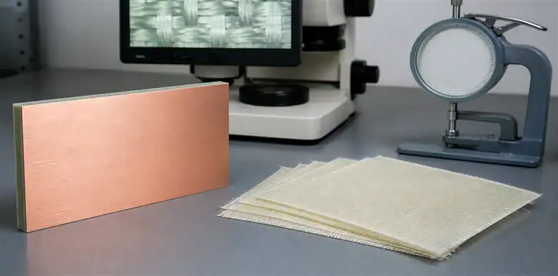
Published dielectric values are not universal constants. A clamped stripline value, split-post resonator result, or design Dk derived from circuit correlation can differ because each method samples the material differently. Frequency, resin content, copper removal, moisture conditioning, and anisotropy also matter. Two suppliers can quote the same branded system yet build simulations around different numeric assumptions.
Create a short model-control table inside the stackup package:
| Input | Buyer record | Supplier response |
|---|---|---|
| Dk value | Value and source revision | Accepted value or proposed correlation value |
| Df value | Frequency and method | Value used for loss prediction |
| Copper model | Foil profile and roughness model | Actual foil family and roughness evidence |
| Dielectric height | Nominal model value | Predicted pressed value and tolerance |
| Temperature | Simulation condition | Qualification or test condition |
The table prevents an apparently small material substitution from silently becoming a model change. It also lets the SI engineer reproduce why the quoted stackup passed. For generated or tool-assisted designs, the same discipline belongs in the code-generated impedance stackup review, where numeric inputs must be traced back to an approved construction.
Do not claim that a lower Dk automatically improves signal integrity. Lower Dk can change trace dimensions and propagation delay, but routing density, manufacturable line width, copper roughness, glass interaction, and connector geometry determine the result. The correct value is the one tied to the intended stackup and validated channel model.
Control glass weave and copper-profile assumptions
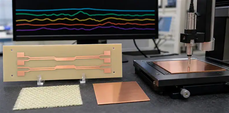
Rogers highlights spread-glass reinforcement and low-profile rolled copper in the RO1200 system. These features address loss consistency and skew mechanisms, but the purchasing package must still identify what will be built.
Glass weave matters because a differential pair can encounter different local ratios of resin and glass. Spread glass reduces severe openings and bundles, yet routing angle, trace pitch, glass style, and resin distribution remain part of skew control. For the most sensitive channels, request the proposed glass construction and check it against the routed geometry rather than writing “spread glass required” without a part-level response.
Copper profile affects conductor loss and effective impedance. A solver that assumes smooth copper can overstate margin if the fabricator buys a rougher foil or applies an adhesion treatment not represented in the model. State whether the selected RO1200 construction uses the published low-profile rolled copper option or another approved foil, and request the foil designation and roughness data needed by the SI model.
The copper roughness and HVLP review is the separate owner for foil terminology and model inputs. In the RO1200 RFQ, link that evidence to each signal-layer copper row. Do not leave one global “HVLP” note that could be interpreted differently for inner and outer layers.
Also examine copper density around critical fields. Large local differences can alter resin flow and pressed thickness. Thieving added by CAM should be governed by approval rules because it can affect plane capacitance, impedance, and skew. The material choice does not remove the need for copper-distribution control.
Build a pressable high-layer-count stackup
Fabrication rule: The approved stackup must balance electrical geometry with resin fill, press cycles, registration, thickness tolerance, and drill aspect ratio.
RO1200 is intended for high-layer-count use, but a high layer count magnifies small construction errors. Several thin bondply interfaces can accumulate more total thickness variation than one model row suggests. Multiple lamination cycles can change dimensional registration and expose interfaces to repeated thermal history. Thick copper or sparse plane regions can demand more resin than the nominal construction supplies.
Require the supplier to review:
- finished board thickness and the tolerance stack behind it;
- core and bondply availability in the chosen construction;
- resin fill around copper features;
- press cycles, foil bonding, and symmetry;
- inner-layer registration and scale compensation;
- drill diameter, finished hole, plating, and aspect ratio;
- backdrill depth and residual stub tolerance where used;
- coupon location and whether it represents the production panel.
| Stackup release field | Required supplier value |
|---|---|
| Dielectric rows | Core or bondply identity, glass style, resin content, pressed thickness |
| Copper rows | Starting foil, plating contribution, finished copper, profile |
| Lamination | Press-cycle allocation, symmetry, predicted total thickness |
| Drilling | Tool size, finished hole, plating, aspect ratio, backdrill residual |
The returned stackup should be a manufacturing record, not a marketing cross-section. It needs layer names that match the Gerber or ODB++ data, controlled impedance classes, finished copper, dielectric construction, material identity, and revision. If the fabricator proposes a change for yield, the response should show the effect on impedance and predicted loss before the buyer approves it.
Do not freeze an impossible nominal thickness. A supplier may need a small dielectric or copper adjustment to meet total thickness and impedance simultaneously. The key is controlled convergence: the fabricator proposes a buildable stack, the SI owner reruns the model, and both parties approve the same revision.
Translate the model into coupon and report requirements
Evidence rule: Match every acceptance record to a property the test can observe, then trace that record to the production panel and material lot.
A successful simulation is design evidence; a coupon and measurement report are production evidence. The RFQ should say which properties are accepted by material certificate, which are checked on a panel coupon, and which require a representative channel vehicle.
Controlled impedance coupons should match the relevant layer pairs, trace geometry, copper process, and dielectric interfaces. Specify target impedance, tolerance, test method, coupon design ownership, report format, and disposition rules. The PCB impedance test report requirements explain what the returned record must identify so a TDR result can be traced to the lot and panel.
Insertion-loss validation needs a separate definition. Name the coupon topology, launch or connector, calibration/de-embedding approach, frequency range, pass limit, and data format. A generic statement such as “test SI” is not actionable. If only first-article coupons are required, distinguish that qualification from routine production inspection.
Material certificates can confirm product identity and lot references, but they do not prove every routed channel. Conversely, one passing coupon does not prove that the correct laminate lot and foil were used. Build an evidence chain:
- purchase and receiving records identify the approved material and lot;
- the traveler links that lot to the production panels;
- the coupon report identifies the panel, layer structure, and test setup;
- deviations are tied to the approved drawing and stackup revision.
This division keeps acceptance proportional. It avoids demanding an expensive full material characterization on every order while preserving proof for the variables that fabrication can change.
| Evidence | Release question it answers |
|---|---|
| Material certificate and receiving record | Was the approved RO1200 construction received? |
| TDR report | Did the manufactured impedance coupon meet its limit? |
| Insertion-loss coupon file | Does a representative route preserve the defined frequency margin? |
| Microsection and dimensional report | Did pressing, registration, drilling, and plating create the approved geometry? |
Manage availability, alternates, and material changes
Change-control rule: Availability pressure may justify an alternate proposal, but it does not turn an unreviewed laminate into an equivalent.
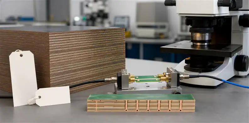
Long lead times, minimum order quantities, regional stocking, foil combinations, or an obsolete glass construction can affect a RO1200 quote. Ask the supplier to state availability at quotation time and identify any material assumption that could change the schedule. A quote based on “or equivalent” should be returned for clarification before tooling starts.
An alternate comparison must include product form, Dk/Df method and frequency, glass style, resin content, copper profile, thickness availability, CTE, Tg or relevant thermal indicators, moisture behavior, flame rating where required, and fabrication history. The SI owner should evaluate geometry and channel loss with the proposed values. Quality and reliability owners should determine whether the change requires coupons, thermal cycling, CAF work, requalification, or customer notification.
Use the PCB material substitution approval workflow to separate a supplier suggestion from an approved baseline. The approval should name the affected part number, lots, stackup revision, validation evidence, and whether the decision is temporary or permanent.
Do not approve a family-level substitute when only one thickness and foil construction were reviewed. A different resin content or foil can change impedance and insertion loss even under the same product family. The smallest controlled unit is the actual construction used in the board.
Release an RFQ that can survive a repeat order
Release rule: Do not issue the production PO until the marked stackup, exception list, and acceptance plan use the same revision as the electrical model.
The final RFQ should let a different engineer reconstruct the decision without relying on a chat message or memory. Include the native fabrication data, controlled drawing, netlist, stackup, impedance table, channel-loss requirement, material callout, copper and glass assumptions, coupon specification, quantity, panel constraints, acceptance rules, and named approval owners.
Ask the fabricator to return a marked stackup and an exception list with the quotation. Silence should not be interpreted as acceptance of every modeled value. Resolve exceptions before a purchase order, then attach the approved response to the released revision.
For repeat orders, preserve:
- approved manufacturer and exact RO1200 constructions;
- laminate, bondply, glass, resin, and foil identities;
- supplier stackup revision and CAM deviations;
- model inputs and channel margin;
- material lot and coupon/report traceability;
- approved alternates and their scope;
- lessons from yield, rework, and reliability results.
The PCB quality documents before shipment page can define the shipment package without turning every certificate into a substitute for engineering validation. When the design and evidence fields are complete, send the controlled package through the QueenEMS contact page for a fabrication review and quote.
Release decision: RO1200 is ready for production only when the supplier’s buildable stackup, the buyer’s electrical model, and the stated acceptance evidence describe the same construction.
FAQ
Is Rogers RO1200 a PTFE laminate?
Rogers positions RO1200 as an extremely low-loss high-speed digital material system. Do not infer resin chemistry or fabrication steps from the loss class alone; use the current product data sheet and fabrication guidance for the exact laminate and bondply construction being quoted.
Can laminate and bondply use one Df value in the model?
Not without an approved correlation. Rogers publishes different maximum Df values for the laminate and bondply at 10 GHz, and the pressed construction contains different resin/glass regions. Use supplier-supported design values for the actual layer interfaces.
Does spread glass eliminate fiber-weave skew?
It reduces severe weave nonuniformity, but routing geometry, trace pitch, glass style, resin distribution, and skew budget still matter. Review critical differential pairs against the proposed construction.
What evidence should accompany the first production lot?
Typical evidence includes material and lot identity, the approved stackup, impedance results, any specified insertion-loss coupon data, dimensional and hole reports, deviation approvals, and shipment-quality records. The exact set should be written into the purchase package.
Sources
- Rogers Corporation, XtremeSpeed RO1200 laminates
- Rogers Corporation, XtremeSpeed RO1200 data sheet
Written by the QueenEMS Engineering Team
Upload your files today · Free DFM check before production · Ship worldwide
Get your PCB prototypes in as fast as 24 hours. We handle FR4, Rogers, and hybrid boards up to 40 layers in volume production, with advanced builds subject to engineering review — free prototypes for 2–4 layer FR-4 boards, no minimum order.
Just upload your Gerber + BOM — we source every part, assemble, and inspect (AOI + X‑Ray) so you don't have to chase suppliers. Boards ship in as fast as 24 hours.