

Quick Answer: To reduce PCB assembly rework, you must demand a First-Pass Yield (FPY) of 99.5%+ for Class 2 boards and enforce strict Design for Manufacturing (DFM) rules. Rework costs multiply rapidly, with a single BGA rework costing $50 to $150 in labor alone, making upfront process controls like 3D SPI and automated reflow profiling mandatory.
Key takeaways:
- Component misalignment, solder opens (34%), and shorts (15%) account for roughly 75% of all factory assembly defects.
- BGA rework carries severe heat damage risks; IPC standards strictly limit BGA component removal to 2 or 3 attempts maximum.
- Optimizing a reflow profile by extending the preheat zone to 120 seconds at 150°C can drop tombstoning rates from 5% to under 1%.
- If your manufacturer returns boards with visible flux residue or refuses to provide AOI defect logs, they have a systematic rework problem.
Table of Contents
- What Are the Most Common PCB Assembly Defects by Industry Statistics?
- How Does Prototype Tombstoning Differ from Mass Production Defects?
- Are Visible Rework Marks on Assembled Boards Acceptable?
- What Are the 8 Root Causes of PCB Assembly Rework?
- How Much Does PCBA Rework Actually Cost Your Project?
- What Is an Acceptable Rework Rate for SMT Manufacturing?
- How Does Design for Manufacturing (DFM) Prevent Rework Before Production?
- What Red Flags Indicate Your CM Has a Systematic Rework Problem?
- What Quality Reports Must You Demand From Your Assembly Partner?
- How to Assess Your CM Using the Buyer-Side Rework Checklist?
You receive a batch of assembled boards, only to find visible flux residue and crooked components. Reworking these defects destroys your delivery timeline and inflates your final unit cost. By forcing your manufacturer to implement strict process controls, you can systematically reduce PCB assembly rework and protect your hardware profit margins. This guide provides buyers with the exact data needed to push back against poor factory quality.
What Are the Most Common PCB Assembly Defects by Industry Statistics?
To reduce PCB assembly rework, you must first target the top three manufacturing defects: solder opens at 34%, solder shorts at 15%, and placement misalignment. These three specific issues combined account for approximately 75% of all surface mount technology (SMT) failures on the factory floor.
Other common defects plague modern high-density boards, driving up manual touch-up times. When components shrink, the margin for error disappears.
- Tombstoning: Small passive components stand on one end due to uneven wetting forces.
- Insufficient Solder: Weak joints caused by blocked stencil apertures.
- Solder Balls: Tiny spheres of solder causing microscopic shorts between fine-pitch pads.
- Cold Solder Joints: Dull, brittle connections resulting from inadequate reflow temperatures.
Here is the reality: If your Contract Manufacturer (CM) does not actively track these specific defect categories, they cannot fix their root causes. You cannot manage what you do not measure.
Bottom line: Demand that your manufacturer categorizes every failure by defect type; if solder opens or shorts exceed 2% of your total placement count, their solder paste printing process is fundamentally broken.
How Does Prototype Tombstoning Differ from Mass Production Defects?
When you attempt to reduce PCB assembly rework, you will notice that tombstoning rarely occurs on prototypes but suddenly spikes in mass production because the thermal profiles are entirely different. Prototypes are often hand-soldered or run in slow, small-batch ovens, whereas production boards speed through massive multi-zone reflow ovens that create severe thermal imbalances.
Real Forum Pain Point: The Prototype vs. Production Shift
Source: Electronics Stack Exchange & EEVBlog Forums Question: “Tombstoning was completely absent in our prototype phase, but our mass production run is suddenly seeing a 5% failure rate. Why did this change, and how do we fix it?”
Answer: Prototype environments cannot replicate the rapid thermal ramping of high-speed mass production. In a large reflow oven, a large copper pour attached to one side of a 0402 resistor acts as a heatsink. One pad melts faster than the other, creating surface tension that pulls the component upright.
You fix this via Reflow Profile Optimization. In a recent Aivon case study, engineers extended the preheat zone to 120 seconds at a stable 150°C. This allowed the entire board to achieve thermal equilibrium before hitting the liquidus phase, dropping the tombstoning defect rate from 5% down to under 1% instantly.
Bottom line: Never assume a successful prototype guarantees a flawless production run; mandate that your CM runs a dedicated thermal profiling board equipped with thermocouples before launching mass production.
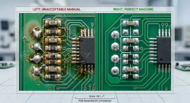
Are Visible Rework Marks on Assembled Boards Acceptable?
To reduce PCB assembly rework disputes, you must understand that visible rework marks are not automatically a failure, but a high frequency of them indicates a failing process. The IPC-A-610 standard allows for manual rework under specific conditions, provided the board passes strict secondary inspections and functional testing.
Real Forum Pain Point: Accepting Reworked Boards
Source: Reddit (r/PrintedCircuitBoard) & All About Circuits Question: “I received my assembled boards and saw visible rework marks (flux residue, slightly different solder joints), but the CM claims all boards passed final test. Is this acceptable?”
Answer: Rework itself is technically acceptable under IPC standards, but the rework rate and rework quality are the true concerns. IPC-A-610 permits manual touch-ups, but it strictly requires mandatory re-inspection of the affected area.
However, if more than 3% to 5% of your total boards show clear signs of manual intervention, your CM likely has a severe, systematic process issue they are trying to hide. Manual soldering degrades pad adhesion and increases the risk of latent field failures.
Bottom line: Accept minor, localized rework on a handful of complex boards, but instantly reject any shipment where more than 5% of the units show visible touch-ups, flux stains, or heat discoloration.
What Are the 8 Root Causes of PCB Assembly Rework?

To reduce PCB assembly rework effectively, you must trace every manual touch-up back to its origin across four categories: design flaws, equipment issues, material problems, and human error. Identifying the exact root cause allows you to force your factory to implement preventive steps rather than reactive fixes.
If you treat every defect as a mystery, you will pay for the same mistakes indefinitely.
| Root Cause Category | Specific Defect Example | How to Prevent at Design Stage | What to Demand from CM |
|---|---|---|---|
| 1. Pad Sizing (Design) | Tombstoning | Balance thermal reliefs on copper pours. | Automated Design Rule Checks. |
| 2. Stencil Aperture (Design) | Insufficient Solder | Adjust aperture-to-pad volume ratios. | 3D Solder Paste Inspection (SPI). |
| 3. Placement Accuracy (Equipment) | Component Shifting | Use highly contrasting fiducial markers. | Regular pick-and-place calibration. |
| 4. Reflow Profile (Equipment) | Cold Solder Joints | Avoid placing tall parts next to micro-chips. | 10-zone minimum reflow profiling. |
| 5. Paste Age (Material) | Solder Balls | Specify paste chemistry limits. | Strict FIFO inventory tracking. |
| 6. Component Oxidation (Material) | Poor Wetting | Designate Moisture Sensitivity Levels (MSL). | Dry cabinet storage tracking. |
| 7. Human Handling (Error) | Fingerprint Contamination | Maximize automated handling clearances. | Mandatory ESD and glove policies. |
| 8. Mask Clearance (Fab) | Solder Bridging | Expand solder mask expansion rules. | Bare board optical inspection. |
Use this table during vendor audits; if a factory cannot show you their SPI machine (solving Cause 2) or their dry cabinets (solving Cause 6), cross them off your list.
Bottom line: Stop blaming the factory for bad pad sizing; you must run a comprehensive DFM review to fix design flaws before blaming the assembly line for equipment or material errors.
How Much Does PCBA Rework Actually Cost Your Project?
Efforts to reduce PCB assembly rework are driven by the Cost Multiplier Effect, where a defect caught at the design stage costs dollars, but a field failure costs thousands. A single BGA rework procedure costs between $50 and $150 in localized labor alone, destroying the profit margin on that specific unit.
Real Forum Pain Point: The Hidden Cost of BGA Rework
Source: SierraConnect & EEVBlog Forums Question: “My CM is charging me excessive fees for BGA rework, and some boards still fail after the fix. Why is this so expensive, and what is the limit?”
Answer: BGA rework is the most expensive manual process in manufacturing. The Rework Cost Calculator concept dictates that the true cost equals the specialized labor rate, plus the severe risk of secondary heat damage, plus the mandatory X-ray re-inspection cost.
A technician must bake the board, use a highly specialized BGA rework station to melt the specific joint without lifting the pad, and re-ball the new component. Furthermore, IPC limits BGA component rework to a maximum of 2 or 3 attempts before the extreme heat permanently damages the fiberglass substrate.
Bottom line: If your factory’s BGA rework rate consistently exceeds 2%, stop paying for manual fixes and immediately switch to a CM that utilizes 3D AOI and SPI to prevent placement errors.
What Is an Acceptable Rework Rate for SMT Manufacturing?

You can confidently reduce PCB assembly rework by demanding industry-standard benchmarks: a First-Pass Yield (FPY) of 99.5%+ for standard Class 2 SMT assemblies, and 99.0%+ for strict Class 3 aerospace boards. If your manufacturer delivers an FPY below 98%, their baseline process controls are fundamentally unstable.
First-Pass Yield (FPY) is the percentage of printed circuit boards that pass all automated and functional tests the very first time without requiring any manual intervention.
What does this mean for you?
- Class 2 (Consumer/Industrial): Allows slight cosmetic imperfections. 99.5% FPY is the expected target.
- Class 3 (Medical/Military): Requires perfect barrel fill and joint integrity. 99.0% FPY is acceptable due to ruthless inspection standards.
- Sub-98% Yield: Indicates severe stencil design flaws or failing pick-and-place nozzles.
Bottom line: Write a minimum FPY guarantee into your manufacturing contract; if the factory cannot maintain a 98% yield, they must absorb all associated rework labor and scrap costs.
How Does Design for Manufacturing (DFM) Prevent Rework Before Production?
Design for Manufacturing (DFM) analyzes your CAD files to prevent 70% of potential defects before a single component is placed. By correcting mismatched pad geometries and applying precise stencil aperture reductions, engineers eliminate the physical conditions that cause solder bridging and tombstoning.
You cannot fix a bad design with good soldering. If your thermal reliefs are unbalanced, the reflow oven will inevitably pull the component off its pad.
Factory Insight: Fixing Bridging Through Stencil DFM
A commercial client experienced a severe 12% shorting rate on a dense 0.4mm pitch QFN component due to their generic CAD footprint. During our free DFM/DFA engineering review, we customized their solder paste layer, applying a 10% volume reduction “window pane” pattern to the center thermal pad. This specific DFM adjustment dropped the bridging defect rate to an acceptable 0.1% instantly, eliminating hours of manual rework.
Bottom line: Refuse to work with any PCB assembly partner who blindly accepts your Gerber files; mandate a formal DFM report that specifically flags risk areas for bridging and insufficient solder.
What Red Flags Indicate Your CM Has a Systematic Rework Problem?
If you want to reduce PCB assembly rework, watch for critical red flags upon delivery: boards arriving with sticky flux residue, visible manual soldering marks on automated components, highly inconsistent solder joint shininess, or a CM who flatly refuses to share their FPY data.
These symptoms reveal a factory that relies on “hidden factories”—teams of technicians manually fixing boards in the back room rather than fixing the automated SMT line.
Factory Insight: Eradicating the Hidden Factory
An IoT startup received prototype boards from a low-cost broker that were covered in heavy flux residue, masking burned FR4 material from clumsy manual touch-ups. They transferred the project to our facility. We transitioned their build to an entirely automated line utilizing 3D AOI feedback loops and strict multi-zone reflow profiling. We achieved a 99.7% first-pass yield, completely eliminating the need for post-reflow manual soldering and eradicating the flux residue issue.
Bottom line: If you easily spot dull, grainy, or flux-stained solder joints next to perfectly shiny ones, your CM is manually patching their mistakes and hiding their true defect rate.
What Quality Reports Must You Demand From Your Assembly Partner?
To verify your CM can reduce PCB assembly rework, you must demand hard data: Solder Paste Inspection (SPI) volume metrics, an Automated Optical Inspection (AOI) defect log complete with failure images, a verified First-Pass Yield (FPY) report, and a detailed rework log assigning a root cause to every touched board.
If a factory claims they have great quality but cannot produce an SPI report, they are guessing at their solder volumes.
Factory Insight: X-Ray Verification
A medical device company suffered sporadic field failures because their previous CM did not X-ray leadless QFN packages, allowing massive solder voids to pass visual inspection. We implemented mandatory 3D X-Ray inspection on every single critical BGA and QFN joint for their next production batch. We caught 4 hidden thermal voids before shipping, saving the client $12,000 in potential field warranty recalls.
| Required Quality Report | What It Proves | When to Demand It |
|---|---|---|
| SPI Volume Data | Proves the stencil design is depositing exact paste amounts. | First Article Inspection (FAI). |
| 3D AOI Defect Log | Shows the exact placement or soldering errors occurring. | Every production batch. |
| FPY Tracking Report | Proves the line runs efficiently without manual fixing. | Monthly vendor review. |
| X-Ray Images | Verifies hidden BGA/QFN joints have minimal voiding. | On every leadless package order. |
Demand the 3D AOI Defect Log explicitly; if it shows constant “false calls,” the factory is not programming their optical equipment correctly.
Bottom line: Stop trusting verbal promises of “high quality”; mandate that your CM includes an itemized rework log and a First Article Inspection (FAI) report with every single shipment.
How to Assess Your CM Using the Buyer-Side Rework Checklist?
Procurement managers must aggressively reduce PCB assembly rework by auditing potential partners before signing a contract. A pristine factory floor means nothing if their internal process control systems allow defects to pass through unrecorded.
Use this 10-point Buyer-Side Rework Assessment Checklist during your next facility audit:
- What is your exact First-Pass Yield (FPY) across standard Class 2 SMT lines?
- Do you use 3D SPI (Solder Paste Inspection) machines before component placement?
- Can you provide a sanitized AOI defect log from a recent production run?
- How many times do your internal procedures allow a BGA to be reworked?
- Do your technicians log the specific root cause for every manually reworked board?
- How frequently do you run external thermal profiling boards through your reflow ovens?
- What is your system for tracking Moisture Sensitivity Level (MSL) components?
- Do you provide a mandatory DFM/DFA review before tooling begins?
- Is 3D X-Ray inspection standard or an extra charge for BGA components?
- If the FPY drops below 98%, what is your formal corrective action procedure?
Bottom line: If a contract manufacturer hesitates, gets defensive, or provides vague answers to more than two of these checklist questions, immediately disqualify them from your approved vendor list.
Defective boards do not happen by accident; they are the direct result of unoptimized pad geometries, careless solder paste printing, and outdated reflow profiles. By shifting from a reactive mindset to a proactive one, you force the manufacturer to prioritize First-Pass Yield over hidden manual touch-ups.
At QueenEMS, we engineer defects out of existence before the machines turn on. Our mandatory, free DFM/DFA engineering review eliminates stencil and pad flaws, while our 3D AOI and X-Ray inspections guarantee joint integrity. With our 99.7% first-pass yield rate and up to 60-layer PCB fabrication capabilities, we deliver flawless turnkey solutions from prototype to mass production scaling.
Stop accepting messy boards and hidden rework costs. Contact us today to experience transparent, data-driven PCB assembly.
Written by the QueenEMS Engineering Team
FAQs
Can I legally reject a PCB shipment if I see manual rework marks on the components? It depends on your contract and the severity. Under standard IPC-A-610 Class 2 rules, manual rework is acceptable if it meets visual and functional criteria. However, if you explicitly contracted for zero-rework, or if the rework caused board delamination or severe flux staining, you have grounds to reject the specific defective units.
What’s the best way to prove my manufacturer caused the tombstoning defect, not my design? You must request their 3D Solder Paste Inspection (SPI) data and their specific reflow oven thermal profile graph. If the SPI shows perfectly even paste volume on both pads, but the thermal profile shows a ramping gradient that is too aggressive, the factory’s oven settings caused the tombstoning, not your CAD footprint.
How do I know if my CM is hiding a high defect rate behind closed doors? Request a comprehensive First-Pass Yield (FPY) report along with the Automated Optical Inspection (AOI) machine’s raw defect log. If the CM claims a 99% success rate but refuses to provide the time-stamped AOI logs showing what failed on the initial run, they are operating a “hidden factory” of manual fixers.
Is it safe to rework a complex BGA component more than once? No, it is highly risky. IPC guidelines strictly limit BGA rework to a maximum of 2 or 3 attempts. Repeated exposure to extreme, localized heat severely stresses the FR4 substrate, leading to lifted pads, internal trace fracturing, and severe reliability issues in the field.
Upload your files today · Free DFM check before production · Ship worldwide
Get your PCB prototypes in as fast as 24 hours. We handle FR4, Rogers, and Flex up to 60 layers — free prototypes for 2–4 layer boards, no minimum order.
Just upload your Gerber + BOM — we source every part, assemble, and inspect (AOI + X‑Ray) so you don't have to chase suppliers. Boards ship in as fast as 24 hours.