
Quick Answer: PCB panelization groups multiple individual boards into a single manufacturing array, typically 18×24 inches, to fit standard assembly conveyor tracks. V-score panelization costs 15–20% less than tab routing and requires a 0.5mm clearance, while tab routing uses 0.8mm mouse bites and requires a 6.4mm clearance for ceramic capacitors.
Key takeaways:
- V-score cuts require leaving exactly 1/3 of the board thickness intact as a structural web.
- Mouse bite breakout tabs should be placed every 1.5 to 3.0 inches along routed edges.
- Maintaining consistent component orientation across a panel cuts SMT pick-and-place time by 10–15%.
- Standard 18×24 inch fabrication panels yield a usable area of 16×22 inches after subtracting process rails.
Table of Contents
- What is PCB panelization and why does every SMT line require it?
- What are standard PCB panel sizes for fabrication and assembly?
- How does V-score panelization work for rectangular boards?
- When should you use tab routing with mouse bites instead?
- What are the golden rules for mouse bite hole size and spacing?
- Can you mix different board designs on one family panel?
- How does depaneling stress damage components near panel edges?
- What is laser depaneling and when does it beat mechanical methods?
- How should you handle X-out boards inside a production panel?
- What DFM rules for rails, fiducials and tooling holes prevent SMT failures?
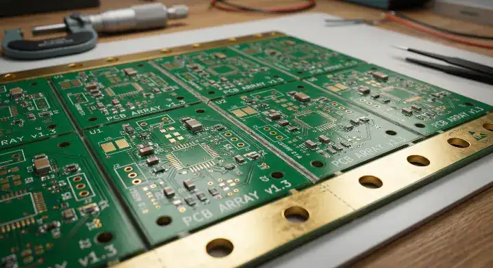
You design a perfect 20x20mm sensor board, but your manufacturer rejects it. Single small boards cannot run through standard surface mount technology lines without falling between the conveyor belts. Panelizing your design solves this physical limitation. Our data at QueenEMS shows an optimized panel layout achieves a 99.7% first-pass yield rate while lowering per-unit production costs.
What is PCB panelization and why does every SMT line require it?
PCB panelization is the process of connecting multiple printed circuit boards into a larger array using breakaway tabs or V-shaped grooves. SMT placement machines require boards to have a minimum width of 50mm to 70mm to clamp securely in the conveyor system. Grouping smaller designs into a single panel satisfies this mechanical requirement and speeds up production.
Consistent component orientation across the panel reduces the distance the robotic head travels. When you face all components in the same direction, our data shows a 10–15% reduction in SMT assembly time. If your design involves wave soldering, you must align the panel’s long edge parallel to the direction of the solder wave flow to prevent solder bridging on fine-pitch ICs.
If your boards are larger than 100x100mm, you might question if panelization makes sense. The reality is, handling a 4-up array of a 100mm board still reduces loading and unloading time by 75% compared to single pieces.
Bottom line: You must panelize any board smaller than 50x50mm, and you should panelize larger boards to cut per-unit assembly costs by 10-15%.

What are standard PCB panel sizes for fabrication and assembly?
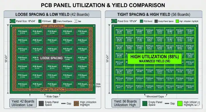
Standard PCB manufacturing panels are typically 18×24 inches (457×610mm) or 12×18 inches (305×457mm). After you subtract the 1-inch mandatory clearance border required for manufacturing clamps and process rails, an 18×24 inch panel gives you a usable routing area of 16×22 inches.
When ordering quick-turn prototype boards, manufacturers prefer the 12×18 inch format. Your goal is to arrange your individual boards to utilize the maximum percentage of this usable area. Wasted FR4 space directly increases your cost per board.
| Panel Size | Usable Area | Best Application | Recommended Board Thickness |
|---|---|---|---|
| 18×24 inches | 16×22 inches | High-volume mass production | 1.6mm – 2.4mm |
| 12×18 inches | 10×16 inches | Prototyping and mid-volume | 0.8mm – 1.6mm |
| 21×24 inches | 19×22 inches | Large backplanes | 2.0mm – 3.2mm |
If you are running a prototype batch, choose the 12×18 inch format. If you are moving to mass production with standard 1.6mm thickness, choose the 18×24 inch format to minimize material waste.
Panel dimensions directly dictate the thermal mass inside the reflow oven. A fully loaded 18×24 inch panel requires a slightly longer pre-heat soak profile than a smaller 12×18 inch array.
Bottom line: Always fit your array into a 16×22 inch usable zone to maximize material utilization on standard 18×24 inch production panels.
How does V-score panelization work for rectangular boards?
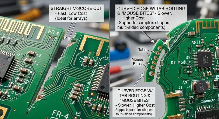
V-score panelization uses a rotary circular saw to cut a V-shaped groove across the top and bottom of the panel, leaving exactly 1/3 of the board thickness intact as a central web. This method costs 15–20% less than tab routing because straight mechanical cuts execute much faster than complex CNC milling paths.
According to guidelines from the SMTA, this “1/3 top, 1/3 web, 1/3 bottom” ratio provides enough structural integrity for the SMT process while allowing easy separation later. You must maintain a minimum copper clearance of 0.5mm from the V-score line to prevent the saw blade from exposing internal ground planes.
Component keep-out zones are equally strict. Standard SMD parts need at least 0.5mm to 1.0mm clearance from the V-cut center. For fragile components, the distance increases significantly.
| Feature | V-Score Panelization | Tab Routing (Mouse Bites) |
|---|---|---|
| Best Board Shape | Strict rectangles and squares | Irregular, circular, overhangs |
| Cost | 15–20% cheaper | Higher cost (longer CNC time) |
| Edge Quality | Rough, exposed fiberglass | Smooth, milled edge (except tabs) |
| Clearance Rule | 0.5mm copper / 1.0mm SMD | 0.5mm copper / 3.2mm SMD |
If your board consists of straight edges and right angles, choose V-scoring. If your board has curved outlines or overhanging connectors, choose tab routing.
Bottom line: Choose V-scoring for square or rectangular boards to save 15-20% on fabrication costs, provided you maintain a 0.5mm copper clearance.
When should you use tab routing with mouse bites instead?
Tab routing with mouse bites uses a CNC router to mill a 2.0mm outline around irregular boards, leaving 3 to 5 small perforated tabs per side to hold the board inside the panel. You should use this method when your design has circular shapes, complex angles, or USB connectors extending past the board edge.
For standard designs, you place a breakout tab every 1.5 to 3.0 inches along the routed edge. This frequency stops the board from sagging in the middle during the high heat of the reflow oven. If you space the tabs too far apart, you exceed typical manufacturing tolerance margins for board flatness.
Hybrid panels combine both techniques. If your board has straight side edges but complex top and bottom edges, manufacturers will V-score the straight lines and use tab routing for the irregular sections.
Are you worried about edge aesthetics? The truth is, tab routing leaves a completely smooth edge around 95% of the board, with only the broken tab areas showing slight fiberglass burrs.
Bottom line: You must use tab routing if your board is not perfectly rectangular or if connectors overhang the PCB outline.
What are the golden rules for mouse bite hole size and spacing?
Based on a common question from Reddit’s r/PrintedCircuitBoard: What size should mouse bite holes be, and how close can I put a 0402 cap to a breakaway tab? The standard mouse bite hole size is 0.8mm in diameter, spaced 1.0mm center-to-center, with 3 to 5 holes per tab. You must keep 0402 ceramic capacitors at least 6.4mm (0.25 inches) away from these breakout tabs to prevent cracking.
If you use smaller 0.5mm holes, the tab becomes too rigid and requires extreme force to break. If you use 1.0mm holes, the tab might snap prematurely inside the pick-and-place machine. The 0.8mm specification offers the best balance of strength and breakability.
| Parameter | Recommended Dimension |
|---|---|
| Hole Diameter | 0.8mm (0.5mm to 1.0mm acceptable) |
| Hole Spacing (Center-to-Center) | 1.0mm |
| Holes Per Tab | 3 to 5 holes |
| Tab Spacing Along Edge | Every 1.5 to 3.0 inches |
| MLCC Capacitor Clearance | 6.4mm (0.25 inches) minimum |
If you are designing the tab structure, choose 0.8mm holes at 1.0mm pitch for standard 1.6mm FR4 boards.
Last quarter, a wearable device client sent us a panel with 0402 MLCCs placed just 2mm from the mouse bite tabs. During our DFM review, we flagged this as a high-risk layout. The client pushed back, saying their previous assembler had no issues. We ran a test batch of 50 panels anyway. After depaneling with our standard router, 8% of the boards showed capacitor failures during thermal cycling — failures that passed initial electrical testing but would have surfaced in the field within 6 months. We re-laid the panel with a 6.4mm keep-out zone for all ceramic passives and the failure rate dropped to zero on the rerun. That single DFM catch saved the client an estimated $12,000 in warranty returns.
Bottom line: Standardize your mouse bites at 0.8mm holes with 1.0mm spacing, and enforce a strict 6.4mm keep-out zone for all ceramic components.
Can you mix different board designs on one family panel?
Answering a frequent Electronics Stack Exchange question: Can I panelize two different PCB designs together to save on setup costs? You can mix designs on a family panel if they share the exact same layer count, 1oz copper weight, 1.6mm board thickness, and ENIG surface finish. Doing this saves you a single $150–$300 NRE setup fee.
For prototype runs (5–10 boards), a family panel saves significant money because NRE fees make up a large percentage of the total bill. For mid-volume (100–500) and high-volume (1,000+) runs, family panels cause extreme waste. If board A requires 1,000 units but board B only requires 200 units, producing the shared panel forces you to build and discard 800 useless copies of board B.
Component height also plays a role. If one board holds tall electrolytic capacitors and the adjacent board has a fine-pitch BGA, the solder paste stencil thickness will conflict.
Bottom line: Choose family panels for early prototype stages to save $150-$300 in setup fees, but separate the designs into independent panels for mass production.
How does depaneling stress damage components near panel edges?
Addressing a major issue discussed on the EEVBlog Forum: We’re getting random failures on 0402 caps near the board edge after depaneling… These failures are latent micro-cracks in Multi-Layer Ceramic Capacitors (MLCCs) caused by the mechanical bending stress of separating the panel. You must increase your component-to-edge clearance to 6.4mm or switch from hand-snapping to a mechanical router.
These micro-cracks are often too small for standard X-ray inspection to detect. The capacitor passes end-of-line electrical testing, but as the device undergoes temperature changes in the field, the crack expands and shorts the component. The IPC-7351B standard directly addresses this by recommending a 6.35mm minimum distance for rigid components.
Hand separation is the primary culprit. When operators manually snap V-scored boards, the bending angle exceeds safe limits and leads to board bowing issues.
Bottom line: Never snap production panels by hand; use a mechanical router or V-score saw to prevent hidden micro-cracks in your ceramic capacitors.
What is laser depaneling and when does it beat mechanical methods?
Laser depaneling uses a highly focused UV or CO2 laser beam to ablate the FR4 substrate, separating the boards with zero mechanical stress and an accuracy of ±25 microns. You should use laser depaneling when your board thickness is under 1.0mm, or when you place ultra-small 01005 components right up against the board edge.
While routers and V-saws apply physical force to the PCB, lasers do not touch the board at all. This makes it the safest separation method available. However, laser cutting is slower and significantly more expensive per panel.
| Depaneling Method | Mechanical Stress | Precision | Best For | Cost Level |
|---|---|---|---|---|
| Laser | Zero stress | ±25 microns | 01005 parts, <1.0mm boards | High |
| Router | Low stress | ±100 microns | Tab routed irregular boards | Medium |
| V-Score Saw | Low to medium stress | ±200 microns | Straight rectangular boards | Low |
| Manual Snap | Extremely high stress | N/A | Cheap prototypes only | Zero |
If your design features 01005 passives near the edge, choose laser depaneling. If you have standard components with proper 6.4mm clearance, choose the cheaper V-score saw.
Dust accumulation is another factor. Mechanical routers create fine fiberglass dust that requires vacuum extraction. Lasers vaporize the material, leaving completely clean edges suitable for medical or aerospace environments.
Bottom line: Specify laser depaneling when you are working with boards thinner than 1.0mm or extremely dense layouts where standard clearance rules are impossible.
How should you handle X-out boards inside a production panel?
An X-out panel is a production array that contains one or more defective sub-boards, typically marked with a physical sharpie cross or a digital “bad-mark” in the machine data. Most assembly houses will process panels containing up to 20% X-outs without charging a penalty, simply programming the pick-and-place machine to skip the marked units.
For a standard 4×4 panel, a 20% allowance means the fabricator can ship arrays with up to 3 defective boards. If you demand “No X-out” panels for your order, the bare board manufacturer will charge a 15–25% premium because they must throw away entire panels if just one small board fails the electrical fly-probe test.
Digital bad marks are the modern standard. The fabricator embeds the failure data into a file that the SMT machine reads, removing the need for a human operator to look for physical sharpie marks.
Bottom line: Accept panels with up to 20% X-outs to save 15-25% on bare board fabrication costs, as SMT machines can easily skip the bad units.
What DFM rules for rails, fiducials and tooling holes prevent SMT failures?
Process rails are sacrificial borders added to the panel, typically 3mm to 5mm wide, that hold the tooling holes and fiducial markers required by the SMT machinery. Tooling holes must be exactly 3.0mm in diameter, unplated, and placed in the corners of the rails to allow the conveyor clamps to lock the panel securely during solder paste printing.
Fiducial markers are 1.0mm bare copper dots surrounded by a 2.0mm solder mask opening. You must place at least three fiducials asymmetrically on the rails. This asymmetric layout prevents the operator from loading the panel backward; if the panel rotates 180 degrees, the camera will fail to register the third fiducial and stop the machine.
A robotics startup came to us with a 22mm × 18mm sensor board — too small for any conveyor system to handle individually. We designed a 4×6 array panel at 160mm × 130mm with 5mm process rails, three asymmetric fiducials, and a hybrid separation approach: V-score on the straight long edges and tab routing with 0.8mm mouse bites on the short edges where a flex cable connector hung over the board outline. The result: 24 boards per panel, 99.7% placement accuracy on their 0.4mm-pitch QFN, and a 15% reduction in SMT cycle time compared to their prototype run at a previous vendor where boards were placed individually. Total per-unit cost dropped from $4.20 to $2.85 — a 32% saving driven entirely by panel optimization.
If you skip these rules, your panel will fail a standard manufacturability design check and stall on the production floor.
Bottom line: Add 5mm process rails, 3.0mm unplated tooling holes, and 3 asymmetric 1.0mm fiducials to guarantee your panel runs smoothly through any automated SMT line.
Getting your PCB panelization right at the CAD stage eliminates material waste and prevents catastrophic component cracking during depaneling. Whether you use V-scoring for standard rectangles or tab routing for complex outlines, obeying strict clearance rules dictates the survival of your final product.
Frequently Asked Questions (FAQ)
Can I panelize different PCB designs on the same panel?
Yes, but only if they share the exact same layer count, copper weight, board thickness, and surface finish. This is called a family panel and saves you a single $150–$300 NRE setup fee. Avoid family panels in mass production because unequal demand for each design wastes material. Always double-check your BOM quantities before requesting a family panel layout.
What’s the minimum distance between a 0402 capacitor and a mouse bite tab?
At least 6.4mm (1/4 inch) is strictly required. Ceramic capacitors are brittle and will crack from the depaneling vibration if placed too close. While standard components can be as close as 3.2mm (1/8 inch), MLCCs need the extra clearance to prevent latent micro-cracks that cause field failures. Review your CAD layout and move any edge-adjacent capacitors today.
How do I choose between V-score and tab routing for my panel?
Use V-score for rectangular boards with no edge-hanging components, as it is 15–20% cheaper and faster. Use tab routing for irregular shapes, round boards, or designs with connectors extending past the board edge. If your board has a complex outline, contact your manufacturer to request a hybrid panelization strategy.
What is the standard PCB panel size for SMT assembly?
The standard size is 18×24 inches (457×610mm) for most SMT lines. After subtracting the mandatory 1-inch borders for process rails, your usable area is about 16×22 inches. Smaller 12×18 inch panels are common for prototypes. Always verify the maximum conveyor width with your assembly partner before locking in your panel dimensions.
Can I snap PCB panels apart by hand instead of using a depaneling machine?
No, hand-snapping is highly discouraged for production boards. Manual separation creates uncontrolled mechanical stress that cracks solder joints and ceramic capacitors near the break point. Hand separation is acceptable only for cheap prototypes with no components within 10mm of the break line. Always specify a V-score saw, router, or laser depaneler for your production runs.
Getting your PCB panelization right at the CAD stage eliminates material waste and prevents catastrophic component cracking during depaneling. Whether you use V-scoring for standard rectangles or tab routing for complex outlines, obeying strict clearance rules dictates the survival of your final product.
QueenEMS provides free DFM/DFA engineering reviews on every order to catch panelization errors before they hit the floor. From prototype scaling to high-volume mass production, our turnkey service handles fabrication, SMT assembly, and stress-free mechanical depaneling. Check out our full capabilities or contact us for a free review of your panel layout.
Written by the QueenEMS Engineering Team
{ “@context”: “https://schema.org”, “@type”: “Article”, “headline”: “PCB Panelization: V-Score vs Tab Routing Rules That Cut Waste by 20%”, “author”: { “@type”: “Organization”, “name”: “QueenEMS” }, “datePublished”: “[发布日期]”, “dateModified”: “[修改日期]”, “publisher”: { “@type”: “Organization”, “name”: “QueenEMS”, “logo”: { “@type”: “ImageObject”, “url”: “https://www.queenems.com/wp-content/uploads/2026/02/cropped-Logo-270×270.jpg” } } } { “@context”: “https://schema.org”, “@type”: “FAQPage”, “mainEntity”: [ { “@type”: “Question”, “name”: “Can I panelize different PCB designs on the same panel?”, “acceptedAnswer”: { “@type”: “Answer”, “text”: “Yes, but only if they share the same layer count, copper weight, board thickness, and surface finish. This is called a family panel and saves one NRE setup fee ($150–$300). Avoid family panels in mass production because unequal demand for each design wastes material.” } }, { “@type”: “Question”, “name”: “What’s the minimum distance between a 0402 capacitor and a mouse bite tab?”, “acceptedAnswer”: { “@type”: “Answer”, “text”: “At least 6.4mm (1/4 inch). Ceramic capacitors are brittle and crack from depaneling vibration. Standard components can be as close as 3.2mm (1/8 inch), but MLCCs need the extra clearance to prevent latent micro-cracks that cause field failures.” } }, { “@type”: “Question”, “name”: “How do I choose between V-score and tab routing for my panel?”, “acceptedAnswer”: { “@type”: “Answer”, “text”: “Use V-score for rectangular boards with no edge-hanging components — it’s faster and 15–20% cheaper. Use tab routing for irregular shapes, round boards, or designs with connectors extending past the board edge. A hybrid approach works when only some edges are straight.” } }, { “@type”: “Question”, “name”: “What is the standard PCB panel size for SMT assembly?”, “acceptedAnswer”: { “@type”: “Answer”, “text”: “Most SMT lines use 18×24 inch (457×610mm) panels. After subtracting 1-inch borders for process rails, the usable area is about 16×22 inches. Smaller 12×18 inch panels are common for prototypes. Always confirm with your assembly partner — their conveyor width sets the limit.” } }, { “@type”: “Question”, “name”: “Can I snap PCB panels apart by hand instead of using a depaneling machine?”, “acceptedAnswer”: { “@type”: “Answer”, “text”: “Not recommended for production boards. Hand-snapping creates uncontrolled stress that cracks solder joints and ceramic capacitors near the break point. Use a V-score saw, router, or laser depaneler. Hand separation is acceptable only for prototypes with no components within 10mm of the break line.” } } ] }Upload your files today · Free DFM check before production · Ship worldwide
Get your PCB prototypes in as fast as 24 hours. We handle FR4, Rogers, and Flex up to 60 layers — free prototypes for 2–4 layer boards, no minimum order.
Just upload your Gerber + BOM — we source every part, assemble, and inspect (AOI + X‑Ray) so you don't have to chase suppliers. Boards ship in as fast as 24 hours.