
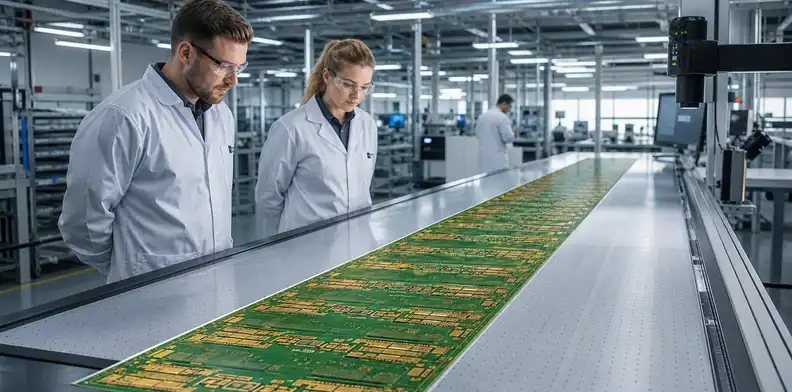
Quick Answer: Extra-long PCB manufacturing is feasible only when the finished outline, layer count, laminate, thickness, copper weight and process tolerances fit one qualified route. A supplier may handle a long two-layer board but not the same outline as a tightly registered multilayer. Send the complete data package and ask for a process-by-process size disposition before freezing the design.
Extra-long PCB manufacturing starts where a board no longer fits the supplier’s routine imaging, lamination, drilling, plating, routing, test or handling window. The governing boundary is not one universal length. It is the smallest usable envelope across every process required by the actual construction.
That distinction matters to engineers sourcing one-meter LED boards, industrial backplanes, power-distribution boards and long control panels. A headline maximum can describe one route while the quotation silently assumes another. This article shows how to turn an unusual outline into a buildable, reviewable manufacturing plan.
Table of Contents
- Define extra-long before requesting a quote
- Check every process envelope, not one machine
- Match construction to the available route
- Control registration and dimensional movement
- Plan copper balance, flatness and support
- Separate bare-board and assembly limits
- Build inspection and electrical test into the route
- Release an extra-long PCB with a written disposition
Define extra-long before requesting a quote
Decision point: A board becomes extra-long when at least one required process can no longer use the supplier’s standard production panel and standard handling method.
Do not define the project only as “about one meter.” Record finished length and width, finished thickness, layer count, material family, copper by layer, minimum features, hole technology, surface finish and quantity. Also distinguish the finished board from removable rails or a customer-controlled panel. A 980 mm finished board inside a 1,020 mm carrier is not the same request as a 980 mm production panel.
Rigid, flex, rigid-flex and metal-backed boards use different processes. Search results for “ultra-long PCB” often mix all four, creating misleading comparisons. A roll-to-roll flex capability does not prove that the supplier can press and register a rigid multilayer of the same length.
Use the Large Format PCB manufacturer page to submit the actual outline and layer count for a route review. The published standard envelope is a starting point, not approval for every combination.
| Input | Why it changes the route | What the supplier should return |
|---|---|---|
| Finished outline and panel outline | Determines usable process field and edge allowance | Confirmed finished and production dimensions |
| Layer count and stack-up | Adds lamination and registration limits | Proposed construction and press route |
| Copper and feature rules | Changes etching, plating and resin behavior | Manufacturable rule set and exceptions |
| Quantity and delivery target | Changes tooling, test and handling economics | Prototype and repeat-production route |
Check every process envelope, not one machine
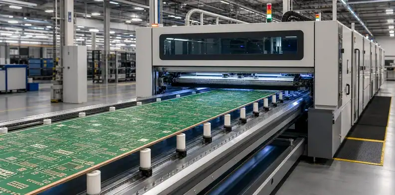
Bottom line: The maximum buildable size is the minimum qualified envelope across material cutting, imaging, lay-up, lamination, drilling, plating, solder mask, finish, routing, test and transport.
A supplier may own a large drill but still have a smaller exposure, press opening or flying-probe field. Conversely, a board may physically enter a machine but leave too little edge area for tooling holes, coupons, plating contact or registration targets. “It fits” is not the same as “it is qualified.”
Ask for a written matrix instead of a single maximum-size number. Each row should state the proposed equipment class, usable panel size, required process margin and any special handling. If the board must rotate between operations, confirm that both orientations fit. If two passes or step processing are proposed, ask how alignment and overlap are controlled.
LPKF’s panelization guidance identifies the machines used at each production stage as constraints on panel dimensions. For this long rigid board, the proposed matrix must cover the actual fabrication sequence and support format, not a length advertised for a different construction.
The PCB stack-up design article explains how construction changes the manufacturing route. For the unusual outline itself, use the pillar page and supplier disposition as the source of truth for the project.
Reject a capability statement that names only the largest machine while omitting the other required operations.
Include wet-process tanks and material transport in the review. A panel that fits the nominal rack may still flex, trap chemistry or contact adjacent hardware when its mass and aspect ratio are unusual. Ask whether the quoted route has been used for a comparable construction and which first-panel checks validate it. Comparable means similar outline, thickness, layer count and copper—not merely another board described as “large.”
Capacity also includes scheduling. Large-field equipment may be shared by several special products and have a different maintenance or batching cycle. Confirm the production lead-time assumption and whether a repeat order uses the same route. This matters when a prototype is processed manually but the production quote assumes dedicated tooling.
Match construction to the available route
Length, layer count and feature density need a joint review because an added process may introduce a different size, registration or handling constraint.
A long two-layer FR-4 board may avoid multilayer lamination and internal registration. Add eight layers, tight impedance, blind vias or heavy copper and the same outline can move into a different engineering category. Thick copper needs more etch compensation and resin fill. Thin boards need more support. High-temperature or low-loss material may have different stock formats and press behavior.
Use a construction matrix during feasibility review:
| Construction change | Likely constraint | Useful design response |
|---|---|---|
| More layers | Lay-up and layer-to-layer registration | Freeze stack-up early and allow supplier review |
| Heavy copper | Etch, plating, resin fill and flatness | Balance copper and avoid unnecessary extremes |
| Very thin finished board | Handling, mask, routing and shipment | Add removable support or review thickness |
| Fine lines over a long span | Imaging scale and dimensional compensation | Define critical zones and realistic tolerance |
| Special laminate | Sheet availability and press recipe | Approve a named material or controlled equivalent |
Do not solve an equipment limit by changing material or stack-up informally. The supplier stack-up signoff should record dielectric thicknesses, copper, material, impedance assumptions and substitution authority before material release.
Control registration and dimensional movement
Evidence check: A long multilayer needs a compensation plan tied to material behavior, artwork scale, tooling strategy and measured production data.
Laminate expands and contracts during imaging, oxide treatment, lamination and thermal processing. Small percentage changes become larger absolute movement across a long span. The risk is not only a shifted outer outline; it includes annular ring loss, connector-to-hole displacement, mask registration and mating features at opposite ends.
An assumed residual scale error of 100 ppm corresponds to 0.10 mm across 1,000 mm: 1,000 × 100/1,000,000. This illustrates sensitivity only; it is not a laminate property or a process capability. Compare the supplier’s measured end-to-end feature error with the actual mating budget. In a worst-case illustrative budget, 0.10 mm board location error, 0.08 mm connector placement error and 0.12 mm enclosure error already consume 0.30 mm. Confirm the datum scheme and whether these contributions can accumulate in the same direction before assigning tolerances.
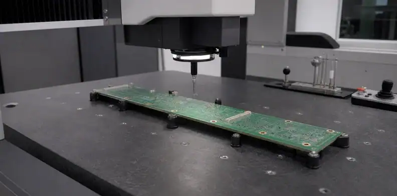
Identify functional datums rather than applying one severe positional tolerance to every feature. Put critical connectors, mounting holes and edge interfaces into controlled datum schemes. Noncritical copper and mechanical features can use general tolerances. This prevents a drawing from forcing an expensive route without improving function.
Ask how the supplier establishes scale factors, how first panels are measured, and what triggers compensation updates. For repeat builds, the approved data revision, material lot and process route should remain traceable. Review the hole-position and datum control process when end-to-end mechanical fit governs acceptance.
Control the relationships that affect assembly and fit; do not substitute a blanket tolerance for a datum strategy.
If the outline and connector datums are already frozen, submit them with the proposed stack-up for an extra-long route feasibility check. The review should return the governing process, open tolerances and first-panel evidence before tooling starts.
Build an end-to-end tolerance budget before tightening the drawing. Include artwork compensation, drilling and routing position, hole/slot size, connector tolerance, assembly placement and enclosure variation. The PCB does not need to consume the complete system budget. When two distant connectors mate independently, define which feature floats and which establishes location; otherwise a nominally precise board can still be impossible to assemble.
Plan copper balance, flatness and support
Key takeaway: Long boards amplify asymmetry, so copper distribution, stack-up symmetry, process support and storage orientation must be planned as one system.
Uneven copper can create different thermal and mechanical behavior across the panel. A stack-up that is electrically correct but mechanically asymmetric may bow after lamination or surface finish. Large solid copper areas on one side and sparse routing on the other can worsen the imbalance. Copper thieving or balancing features may help, but they must respect electrical clearance and customer ownership.
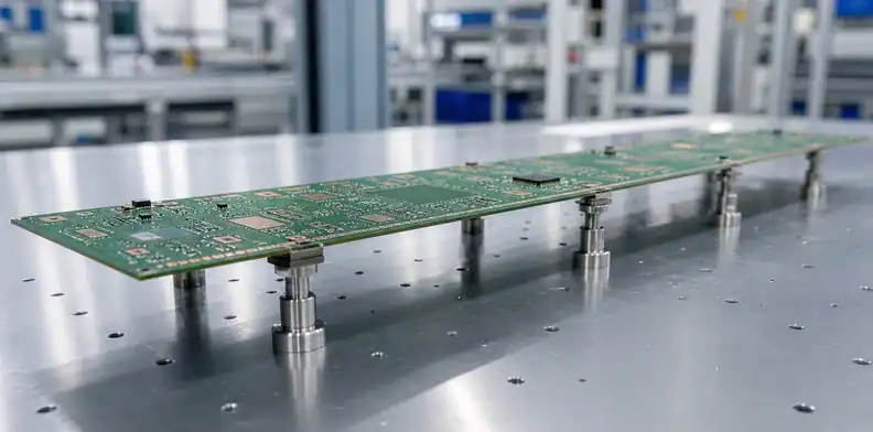
Flatness also depends on how the board is carried. Thin, long panels can sag under their own weight during coating, inspection or assembly. Define permitted support areas and keep-out zones before tooling is designed. Store and transport boards with continuous support rather than resting a thin outline on two distant points.
Specify bow and twist by an agreed method and board condition. Avoid copying a generic percentage into the drawing without checking the product class, connector geometry and assembly process. The PCB bow and twist acceptance article shows how to make the requirement measurable.
Review thermal history as well. A board can pass outgoing flatness and change during baking, soldering or field temperature cycles. If the functional risk occurs after assembly, qualify a representative process condition and include the carrier or fixture used by the assembler. This prevents the bare-board supplier and assembler from measuring different states and reaching opposite conclusions.
Separate bare-board and assembly limits
Decision point: A fabricator’s size approval does not prove that printers, placement machines, reflow conveyors, AOI, fixtures or depaneling equipment can process the assembled board.
If the order includes PCBA, request two dispositions: bare-board fabrication and the full assembly route. Record maximum width between conveyor rails, board length, component height, weight, edge-clearance requirements and permitted support. Check stencil-frame and printer tables, not just placement travel.
Long boards may need carrier fixtures, staged support or a different conveyor direction. A custom carrier can improve repeatability but adds tooling, thermal mass and validation work. Double printing or manual translation of the board is a process change that needs alignment evidence; it should not be an undocumented workaround.
The PCB panelization for assembly article explains downstream rail and equipment interactions. Include the large-board assembly limits directly in the supplier’s controlled route sheet.
Quote fabrication and assembly against the same finished outline, but qualify them as separate equipment chains.
Build inspection and electrical test into the route
What this means: The board is not qualified until the proposed AOI, dimensional inspection and electrical test methods cover the complete usable area.
Ask whether inner- and outer-layer AOI can inspect the panel in one pass and how any stitched or sectional inspection is reconciled. Define the dimensional report around functional datums. For electrical test, confirm probe travel, fixture size, supported board weight and how the panel remains flat during contact.
A large board can be expensive to scrap late, so first-panel evidence is valuable. Typical release evidence may include measured outline and critical feature positions, bow/twist result, impedance coupon data when applicable, electrical-test status and photographs of packaging support. The evidence scope should be agreed before quotation, because it affects panel planning and test time.
Do not ask for every possible report. Ask for evidence tied to a decision: fit, electrical continuity, controlled impedance, flatness or repeatability. That produces a shorter but more useful release package.
For pilot production, define hold points. The supplier might release material after stack-up approval, release the first laminated panel after registration review, and release the lot after dimensional and electrical evidence. Hold points cost time, so use them only where the result can prevent a large batch loss. Once repeat data demonstrates stability, convert selected checks to normal sampling under controlled change rules.
Release an extra-long PCB with a written disposition
Release only after every exception, assumption and special-control step has an owner and an approved revision.
The supplier disposition should list confirmed dimensions, process route, material, stack-up, copper, design-rule exceptions, tooling, test method, flatness requirement, inspection evidence, packaging and delivery assumptions. Separate “confirmed,” “requires customer approval,” “supplier proposal” and “not included.”
Before purchase order, compare the quote to the latest data package. A price based on preliminary dimensions should not be treated as a final build commitment. If the board outline, layer count, copper or material changes, reopen the affected process rows rather than relying on the previous maximum-size answer.
For a usable RFQ structure, follow the PCB fabrication quote-file checklist and add the extra-long route matrix.
The manufacturing claim is complete only when the proposed route, evidence and exceptions can be reviewed without a sales conversation.
Keep the disposition with the approved drawing and purchase order. At repeat order, compare material, panel orientation, process route, tooling and evidence scope against that baseline. A supplier may improve internal methods, but changes that affect the approved construction, functional tolerances or acceptance evidence need the agreed level of customer review.
Frequently Asked Questions
Can a rigid PCB be one meter long?
It can be feasible, but one meter is not a universal standard capability. Layer count, width, thickness, material, copper and the required process sequence determine whether one qualified route exists.
Is a two-layer extra-long PCB easier than a multilayer?
Usually, because it avoids multilayer lay-up and internal registration. It can still be limited by imaging, plating, solder mask, routing, test, handling and shipping.
Can two shorter boards replace one extra-long PCB?
Sometimes. The trade adds connectors, cables, assembly steps and potential failure points. Compare the complete system cost and electrical/mechanical risk, not PCB area alone.
Do extra-long boards always need a carrier?
No. A carrier is needed when thickness, weight, edge clearance or equipment support makes unsupported handling unreliable. The supplier should justify the carrier and identify its effect on thermal processing.
What should I send for a feasibility review?
Send finished and panel outlines, layer count, proposed stack-up, material, thickness, copper, minimum features, drill technology, surface finish, quantities, critical datums, flatness needs and assembly scope.
Written by the QueenEMS Engineering Team.
If your outline is already fixed, request a process-by-process route disposition before committing tooling or laminate.
Check My Extra-Long PCB Route
Upload your files today · Free DFM check before production · Ship worldwide
Get your PCB prototypes in as fast as 24 hours. We handle FR4, Rogers, and hybrid boards up to 40 layers in volume production, with advanced builds subject to engineering review — free prototypes for 2–4 layer FR-4 boards, no minimum order.
Just upload your Gerber + BOM — we source every part, assemble, and inspect (AOI + X‑Ray) so you don't have to chase suppliers. Boards ship in as fast as 24 hours.