
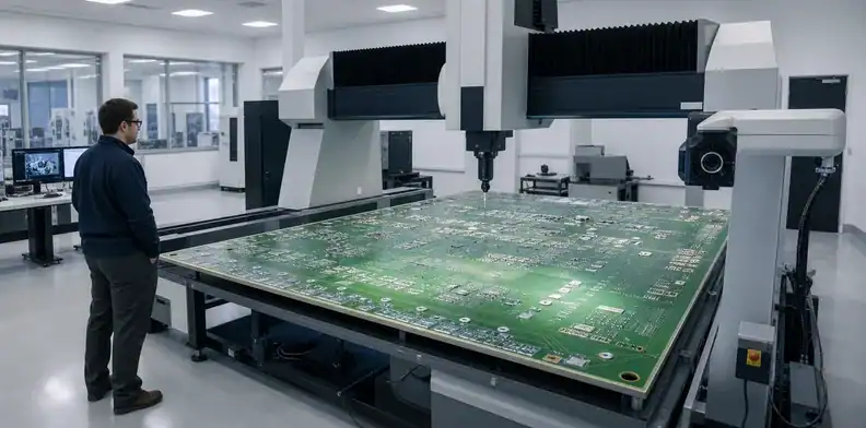
Quick Answer: Large PCB inspection should prove the board fits, lies within the agreed flatness requirement and passes complete electrical coverage. Define finished-board condition, functional datums, measurement method, sampling, equipment field and report format before quotation. A generic “passed inspection” statement is not enough for an oversized board.
Large PCB inspection has to answer more than whether visible defects exist. Long distances magnify datum error, thin panels sag during measurement, and test or AOI equipment may not cover the full outline in one setup. The evidence must show what was measured, how the board was supported and which acceptance rule was applied.
This article shows engineers and buyers how to compare incoming oversized bare boards with the agreed outgoing inspection record. It separates visual inspection, dimensional proof, bow/twist, electrical test and lot records so a supplier can quote the evidence before production begins.
Table of Contents
- Define the inspection condition and acceptance owner
- Verify full-area visual and AOI coverage
- Measure from functional datums
- Control flatness without hiding board sag
- Confirm electrical-test coverage
- Build a useful first-article report
- Set sampling and lot traceability
- Use inspection evidence to release the lot
- Prevent measurement disputes at receiving
Define the inspection condition and acceptance owner
Decision point: Every requirement needs a named board condition, method, limit and decision owner.
Start with the finished product: bare board or assembled board, individual outline or customer panel, room condition or defined preconditioning. Record whether removable rails remain attached and whether the board is measured freely, on a support plane or in a functional fixture. These choices can materially change the result.
Record the board state before comparing outgoing and incoming results. IPC-TM-650 2.4.22 addresses rigid boards and panels; it does not cover the special effects of component weight, supports and connectors on assemblies. A populated board therefore needs an agreed setup appropriate to its function. For a non-rectangular bare board, the method’s enclosing-rectangle approximation can understate deformation. Keep the sample identity, measurement direction and setup photographs with the disputed result, and agree on the method before either party substitutes a fixture-fit check.
The customer drawing should own product-specific limits. A named IPC method can define how to measure, but it does not replace the need to state the applicable product requirement. IPC publishes the IPC-TM-650 Test Methods Manual, including methods used by the industry to evaluate printed-board characteristics.
The large-format capability page lets you check whether the proposed inspection and test fields cover the intended outline. Equipment capacity is part of the acceptance plan, not an afterthought.
| Requirement | Define before quote | Evidence expected |
|---|---|---|
| Visual condition | Product class, defect criteria, full-area coverage | AOI/visual status and exceptions |
| Dimensions | Datums, critical features, tolerance and setup | Coordinate report or first-article table |
| Bow and twist | Board condition, method, limit and support | Measured values and setup record |
| Electrical test | Netlist source, coverage and test method | Pass record with lot identity |
Verify full-area visual and AOI coverage
Evidence check: “AOI passed” is meaningful only when the equipment field, inspection recipe and panel orientation cover the complete product.
Inner-layer AOI should occur before lamination, when shorts, opens, nicks and registration targets remain accessible. Outer-layer inspection should cover finished conductor geometry before mask obscures features. For an oversized panel, ask whether the camera stage scans the full length, whether the board is indexed in sections and how overlap zones are handled.
Sectional inspection can be valid, but the record should identify each region and preserve one product identity. Repositioning must not leave an uninspected stripe or double-count defects. If manual visual inspection supplements AOI at edges or unusual cutouts, list those zones explicitly.
Bare-board conductor AOI and assembled-board AOI inspect different features. The AOI, X-ray and ICT comparison explains their defect coverage. For a large outline, also verify that the selected machine and inspection program can cover the entire board.
The inspection report should map one result to every region of the released outline.
Inspection sensitivity must also match the design. A recipe proven on ordinary line widths may not resolve the narrowest conductor or smallest spacing in the new board. Confirm defect classes, reference data and review thresholds. When the board is scanned in multiple regions, keep the same calibrated sensitivity or document why a region uses a different rule.

Measure from functional datums
Bottom line: A large coordinate report should prove the relationships that control enclosure fit, connectors and tooling—not just overall length and width.
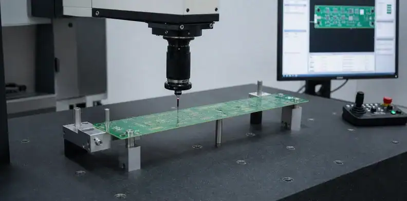
Define primary, secondary and tertiary datums that constrain the board without overconstraining it. Typical choices include a mounting-hole pattern, a routed edge and a critical connector axis. State whether holes are measured at finished diameter and whether edge copper, bevels or slots have separate controls.
End-to-end distance is especially sensitive on a long board. Instead of placing unrelated ordinate dimensions from several origins, use one controlled datum scheme and identify critical characteristics. A supplier can then select a CMM, vision system or calibrated fixture with a field and uncertainty appropriate to those features.
Record the measurement setup: board orientation, support points, temperature when relevant, instrument identification and drawing revision. The PCB hole-position and datum article provides a broader datum-control workflow.
| Characteristic | Weak evidence | Useful evidence |
|---|---|---|
| Overall outline | “Size OK” | Actual L/W, tolerance, method and revision |
| Connector spacing | Screenshot | Measured coordinates from named datums |
| Hole pattern | Go/no-go note | Feature report plus gauge/fixture identity |
| Routed edge | Visual pass | Profile result at defined inspection points |
Control flatness without hiding board sag
In practice: Bow and twist measurement must distinguish board deformation from unsupported gravitational sag and fixture force.
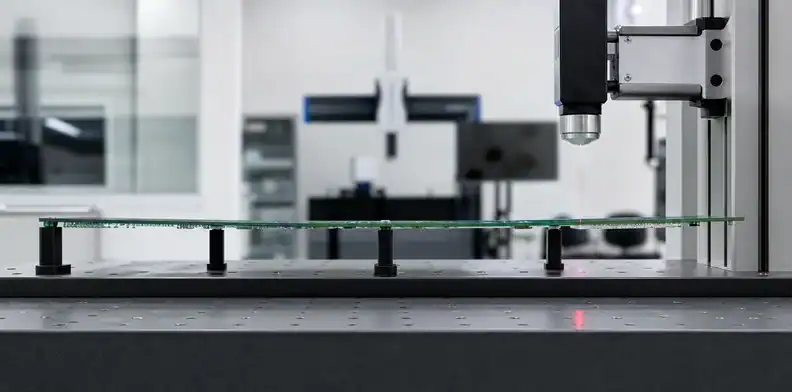
A thin, long board may deflect when two distant points carry its weight. Excessive clamping can create the opposite error by forcing a warped board flat. Agree on the measurement method, support plane, orientation and board condition. Photographs of the setup can be more valuable than a table of unexplained percentages.
Measure the correct object. A customer panel with breakaway rails can be flatter than the finished board after depaneling, while an individual board may behave differently after thermal exposure. If the functional concern is connector coplanarity or enclosure fit, add the relevant feature measurement instead of assuming one global bow/twist number proves everything.
The PCB bow and twist acceptance workflow explains how to connect the requirement to evidence. For an oversized board, also document support spacing and edge condition.
A result without board condition and support setup cannot resolve a receiving dispute.
When supplier and receiving teams use different support setups, send both methods with the drawing and request a measurement-plan review before production. The useful output is one reproducible condition, not two pass/fail certificates that cannot be compared.
Use actual values, not only pass/fail. Actual measurements reveal drift and allow the customer to compare outgoing and incoming condition. Record the maximum deviation, calculation inputs and where it occurred. A repeated high point near the same copper-heavy zone suggests a process pattern; scattered receiving-only damage suggests a different investigation.
If a functional fixture is used, preserve its drawing and calibration logic. A fixture can be an excellent product-level check, but it should not hide which datum or contact caused a failure. Combine fit confirmation with a diagnostic measurement plan so disputes do not depend on one opaque go/no-go result.
Confirm electrical-test coverage
Decision point: Electrical proof must cover the released netlist and fit the board, probes and support system used for the actual outline.
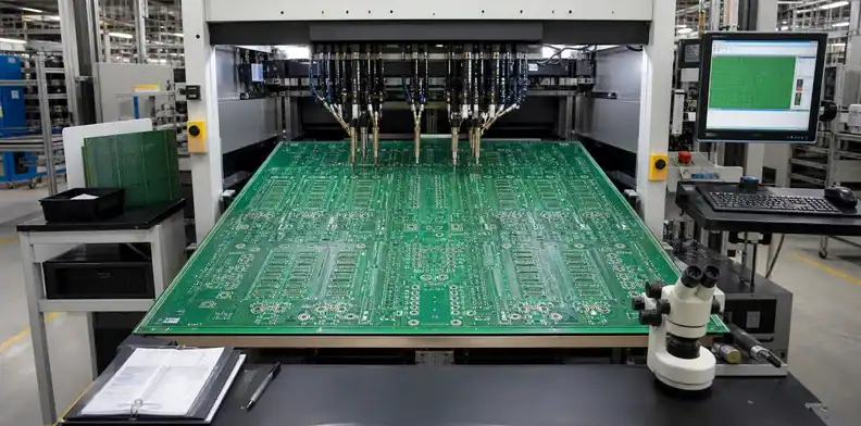
Flying probe is attractive for prototypes because it avoids a dedicated fixture, but probe travel and panel handling still have limits. A bed-of-nails fixture can support production volume but adds tooling, storage and change-control cost. Ask which method is quoted, whether the complete netlist is tested and how the board stays flat during probe contact.
Test data should come from a controlled netlist or approved CAM output, not from an unrelated earlier revision. Define whether the record is a lot-level pass summary, serialized result or detailed failure log. For controlled impedance, electrical continuity does not replace coupon or test-report evidence; use the PCB impedance test report requirements when applicable.
Ask how repaired or retested boards are identified. A final pass may be acceptable, but the disposition and traceability should be visible when the customer requires it.
Open/short thresholds, isolation voltage and test speed should follow the product requirement and equipment capability. Avoid importing a test voltage from a different product without checking clearances and intended service. If the board includes intentionally isolated nets, embedded components or unusual shielding structures, make sure the test program understands them rather than treating every exception as a defect.
Build a useful first-article report
Record rule: The first article should contain enough actual values and setup context to approve the route, not merely repeat drawing tolerances.
Select characteristics that validate process risk: finished outline, critical datum relationships, representative holes and slots, finished thickness, bow/twist, surface finish, impedance when specified and electrical-test status. Add high-resolution images only where they support a decision.
The first-article report should identify part number, revision, lot, material, panel identity, instrument or fixture and inspector/date. Mark deviations and supplier proposals separately from accepted results. If a dimension is not measurable with the proposed equipment field, resolve that before production rather than leaving a blank cell.
The general PCB first-article inspection versus AOI article explains why the two records are not interchangeable. Large PCB inspection needs both route validation and complete defect coverage.
Approve the manufacturing route only after actual results demonstrate the critical long-distance relationships.
Set sampling and lot traceability
What this means: Sampling should reflect the characteristic, process stability and consequence of escape; one sample plan does not suit every check.
Electrical continuity may be required on every board, while detailed dimensional reports may use first-off plus defined lot sampling. Visual inspection can combine automated full-area coverage with manual verification. Bow/twist sampling should consider panel position because edge and center images can behave differently.
Define the production lot and retain links among laminate batch, traveler, panel, test record and shipment. If multiple process routes or panel orientations are used in one purchase order, identify them separately. A combined certificate can hide meaningful variation.
Specify record retention and delivery format in the RFQ. A supplier cannot quote an extensive serialized data package after the fact without affecting inspection time and document control.
Use escalation rules for trends that remain within tolerance. Three consecutive lots moving toward the same dimensional edge may deserve process review before a formal reject occurs. Conversely, a single noncritical measurement near a limit does not justify changing the entire route. Trend rules should identify who reviews the data and which changes require customer approval.
Use inspection evidence to release the lot
A lot is ready when required evidence is complete, deviations are dispositioned and the shipped identity matches the inspected identity.
Use a release checklist with required records, responsible owner and status. Confirm that actual measurements are within limits, electrical test is complete, open defects have approved dispositions and packaging protects the inspected condition. If the boards are reworked after inspection, identify which checks must repeat.
Do not accept a generic certificate as a substitute for a contracted report. Certificates are useful summaries, but they rarely show datum setup, flatness support or sectional AOI coverage. Attach the evidence that supports the high-risk decisions.
For a quote-ready package, use the PCB fabrication quote-file checklist and put the large-board inspection matrix directly into the fabrication drawing or RFQ cover sheet.
Every shipped board should trace to the revision and acceptance records used for the release decision.
Prevent measurement disputes at receiving
Bottom line: Supplier and customer should reproduce the same result by using the same datum logic, board condition and method.
Include receiving instructions for unpacking, acclimation, support and inspection timing. A board stored vertically, clamped during measurement or exposed to a different thermal condition may not reproduce outgoing data. Photograph damaged packaging before removing the product when transport deformation is suspected.
When results disagree, compare setup and instrument capability before debating the number. Review drawing revision, units, datum simulation, board orientation, support, calculation method and calibration status. Preserve the disputed sample until both parties agree on disposition.
| Receiving observation | Immediate action | Evidence to preserve |
|---|---|---|
| Crushed or punctured package | Hold unpacking and photograph all sides | Labels, seals and carrier condition |
| Flatness result differs | Recreate the agreed support and acclimation | Setup photo, actual values and instrument ID |
| Critical feature is out | Confirm revision and datum simulation | Drawing, coordinate report and sample identity |
| Electrical failure appears | Quarantine the affected lot | Netlist revision, tester result and board serial/position |
The table turns a disagreement into a reproducible comparison. It also prevents receiving damage and manufacturing nonconformance from being mixed into one vague rejection.
Receiving inspection should be proportional to risk. New routes and early lots may justify more measurement; stable repeat lots can use reduced verification if change control and supplier data remain reliable. Any material, stack-up, panel orientation or equipment change should trigger the agreed requalification level.
Create one discrepancy form that both parties can use. It should record shipment identity, sample position, measurement setup, actual result, photographs, immediate containment and proposed disposition. A shared evidence format shortens root-cause review and prevents screenshots or informal email descriptions from becoming the only record.
Agree a review milestone for the inspection plan based on the first-lot risks and subsequent production results. Remove evidence that never supports a decision, strengthen checks that reveal drift, and confirm that instruments still cover the released outline. This keeps the package useful rather than allowing it to grow into a costly archive of unread reports.
FAQ
What should large PCB inspection include?
At minimum, define full-area visual/AOI coverage, critical dimensions from functional datums, bow/twist or flatness when required, complete electrical test and lot traceability.
Can standard AOI inspect an oversized PCB?
Only if its stage, optics and recipe cover the full outline. Sectional scanning can work when overlap, region identity and defect reconciliation are controlled.
Is flying-probe testing practical for a large PCB?
It can be, especially at low volume, but probe travel, board support, test time and netlist control must be qualified for the exact outline.
Should every dimension appear in the first-article report?
Not necessarily. Report the characteristics that validate function and process risk, while ensuring all drawing requirements remain subject to the agreed inspection plan.
How do I specify flatness evidence?
Name the board condition, measurement method, acceptance limit, support setup, sampling and report format. Add feature coplanarity or fixture-fit checks when those drive function.
Written by the QueenEMS Engineering Team.
Send your drawing, datum scheme and required evidence to confirm the inspection route before the quote is released.
Review My Large PCB Inspection Plan
Upload your files today · Free DFM check before production · Ship worldwide
Get your PCB prototypes in as fast as 24 hours. We handle FR4, Rogers, and hybrid boards up to 40 layers in volume production, with advanced builds subject to engineering review — free prototypes for 2–4 layer FR-4 boards, no minimum order.
Just upload your Gerber + BOM — we source every part, assemble, and inspect (AOI + X‑Ray) so you don't have to chase suppliers. Boards ship in as fast as 24 hours.