
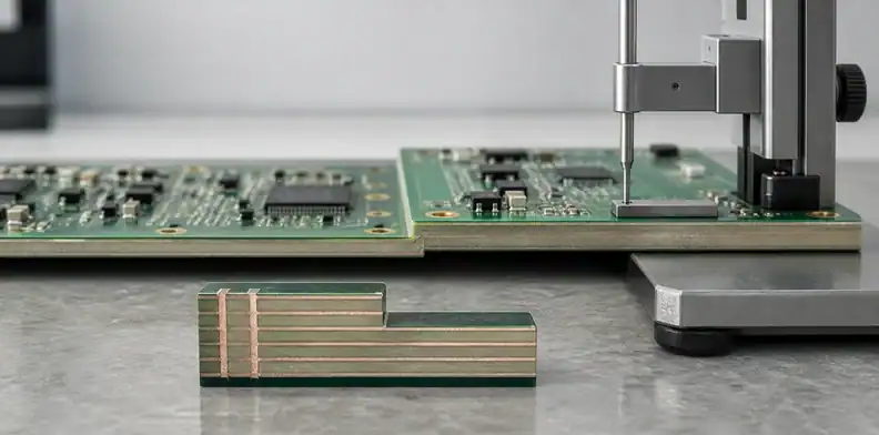
Quick Answer: A stepped-thickness PCB needs a separate layer stack, finished thickness, outline and transition definition for every zone. The RFQ must also state which copper layers continue across each boundary, how the step is formed, what surfaces and datums control assembly fit, and how depth and local thickness will be inspected. One global board-thickness note cannot describe a panel with multiple Z-axis constructions.
Stepped boards solve packaging problems that a uniform panel cannot. One region may need a thin edge under a connector, another may need extra thickness for stiffness, or a local island may carry more layers than an adjacent area. That flexibility creates a fabrication-data problem: conventional drawings often show one stack-up and leave the supplier to infer the rest.
The safest quotation starts with zones. Each zone gets an explicit construction, and every boundary gets a functional explanation and measurable geometry. This prevents a supplier from treating a multilamination structure as ordinary controlled-depth milling or from removing a layer that was intended to carry a signal across the transition.
Table of Contents
- Confirm which kind of stepped board is intended
- Map every stackup zone and continuing layer
- Dimension the transition from functional datums
- Choose the fabrication route before pricing
- Control lamination, resin fill and local thickness
- Protect electrical behavior across the boundary
- Inspect depth, flatness and assembly fit
- Approve changes without breaking zone intent
- Build a quote-ready stepped-board package
Confirm which kind of stepped board is intended
Architecture rule: Identify whether the local height comes from selective plies, machining, a cavity, an insert, or a combined route before comparing quotations.
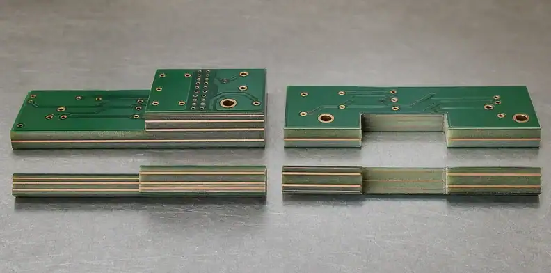
“Stepped PCB” can describe several constructions that look similar in a mechanical model but are fabricated differently. The thick region may contain additional rigid layers laminated only in one zone. A uniform multilayer may be milled after lamination to create a recessed area. A rigid-flex board may expose a thin flex section between rigid islands. A separate stiffener or metal insert may create local height without changing the electrical stack.
Classify the design before asking for price:
- Zone stack-up: different areas contain different layer counts or dielectric builds.
- Machined recess: one common stack is selectively removed to a controlled depth.
- Rigid-flex transition: continuous flex layers remain while rigid material is removed.
- Local stiffener or insert: an added part changes height or support.
- Embedded cavity or coin: a local internal feature changes Z-axis construction.
Each type has different constraints for lamination, routing, copper continuation, edge condition and inspection. If the requirement is only a machined pocket, the existing controlled-depth routing requirements may be the correct owner. This article applies when multiple stack-up zones or a true stepped construction must be communicated and accepted.
Record the functional reason for each height. Connector seating, enclosure clearance, local stiffness, thermal contact and component Z-height create different datum and tolerance needs. The function prevents a supplier from simplifying the construction in a way that preserves appearance but loses performance.
Map every stackup zone and continuing layer
Create a zone table that identifies layer count, layer names, copper weights, dielectric materials, nominal thickness and finished thickness for every region. Use consistent layer identifiers across the table, artwork and cross-section drawing.
The critical question is which layers continue. A copper layer can terminate at the step, continue through both zones, or change its reference relationship. Mechanical CAD may show the thickness change without showing this electrical intent.
For each boundary, state:
- zone names and coordinate extents;
- layers present in each zone;
- layers continuous across the boundary;
- terminated copper and required clearances;
- local dielectric and finished thickness;
- plated or unplated holes that cross the transition;
- controlled impedance or high-current features nearby;
- surfaces used by assembly or enclosure datums.
IPC-2581C includes stackup-zone and Z-axis data elements, which can carry this intent in intelligent manufacturing data. If Gerber and drawings are used instead, provide the equivalent information explicitly.
Use the PCB stack-up design review for the electrical logic inside each zone. Then add the zone map that explains how those local stacks form one manufacturable board.
Dimension the transition from functional datums
Datum check: Step position and height must reference the mating or assembly surfaces that determine function, not an arbitrary panel edge alone.
The transition needs X-Y position, shape, corner condition, slope or vertical-wall intent, local radii and Z-axis values. Dimension it from datums used by the mating connector, component or enclosure rather than from an arbitrary panel edge.
Include cumulative manufacturing allowances. Routing tool diameter creates an inside radius. Lamination and material movement affect where local plies end. Removal operations have depth and surface variation. Final profiling can release stress and change the relationship between zones.
Avoid ambiguous notes such as “thin area 0.8 mm” or “remove to Layer 4.” State whether the 0.8 mm is measured before or after surface finish, whether copper is allowed on the floor, which physical interface defines Layer 4, and what tolerance applies at the transition.
A dimensioned section should show:
- top and bottom finished surfaces by zone;
- local layer sequence and terminated plies;
- transition width and corner radius;
- nominal and tolerance-controlled heights;
- copper and mask keepouts;
- any exposed dielectric, copper or plated wall;
- assembly datum and mating part relationship.
When a fastener or countersunk head crosses zones, coordinate the section with the PCB countersink hole requirements. Do not let two separate mechanical notes create incompatible depth references.
Choose the fabrication route before pricing
Different routes can create the same nominal step but not the same layer continuity, edge quality, tolerance or cost. The supplier should return a proposed process flow before the quotation is treated as technically comparable.
Possible routes include selective-ply lay-up, pre-routed cores or prepregs, sequential lamination, controlled-depth routing, removable window structures, local stiffener bonding or combinations of these. The chosen route determines tooling, material utilization, press cycles, inspection access and repair options.
Compare routes against the product requirement:
| Decision | Route-sensitive question |
|---|---|
| Continuous electrical layers | Can the selected plies cross the step without damage or unsupported copper? |
| Tight local thickness | Is thickness set by cured laminate, machining, grinding or an added part? |
| Clean exposed floor | Will resin, glass fibers, copper or tool marks remain after opening? |
| High volume repeatability | Does the route rely on manual removal or individually matched inserts? |
| Controlled impedance | Does the reference plane and dielectric stay defined through the transition? |
| Assembly fit | Which finished operation establishes the mating surface? |
Do not approve the lowest price before this route is known. One supplier may quote a true multizone lamination while another assumes a post-lamination pocket. The difference can change reliability, tolerance, and cost because the two routes create different layer transitions and inspection needs, even if both use the phrase “stepped board.”
Control lamination, resin fill and local thickness
Thickness rule: Each zone needs its own finished-thickness target and tolerance together with the process that creates its final surface.
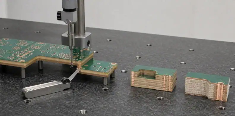
Zone constructions create uneven pressure and resin demand. Thick and thin areas may heat and consolidate differently; ply edges can form resin-rich or resin-starved regions; a local cavity can concentrate pressure or leave unsupported material.
The lay-up plan should identify where each core and prepreg ends, how edges are tooled, how vacuum reaches local features, and how pressure is distributed. Material choice must provide enough resin for copper topography and local fill without flooding an exposed zone or moving the boundary.
Local thickness is not independent from total panel flatness. An asymmetric step can create residual stress, especially when copper density and dielectric construction differ strongly across the board. Review panel orientation, copper balance, cooling and final profiling. Apply the PCB bow and twist acceptance globally and add local surface measurements where the assembly needs tighter control.
For a first article, require sections through representative boundaries. The section should identify the zone, layer endings, resin condition, copper clearance and measured Z-axis values. Select both a simple transition and the most difficult corner or narrow feature.
If a metal insert is part of the step, use a separate controlled insert drawing and acceptance package. The insert introduces bonding, void and coplanarity controls beyond ordinary zone lamination.
For example, a drawing might define a 0.80 mm local zone beside a 1.60 mm main zone, with a 0.20 mm transition radius and a finished step-height tolerance of +/-0.10 mm. Those values are not universal limits; they show why each dimension, unit, datum, and tolerance must be explicit.
Protect electrical behavior across the boundary
A thickness transition can change impedance, return-path continuity, capacitance, current density and electromagnetic coupling. The electrical review should therefore follow the layers, not the external mechanical shape.
For signals crossing zones, identify the reference plane on both sides, dielectric thickness, copper thickness and any line-width change. Avoid an abrupt plane termination under a high-speed trace unless the design provides an intentional return path. If impedance cannot remain constant, define the allowed transition and how it will be modeled or measured.
Power and ground layers that terminate at the step need clearance and current-path review. Narrow copper necks may carry more current than intended. A local thin zone can also reduce insulation distance or bring copper closer to an exposed surface.
Drilled holes near a boundary deserve special attention. The drill may pass through changing layer support, and a plated barrel can intersect terminated copper or local cavities. Define keepouts, hole start and stop layers, and inspection sections. Do not allow CAM to delete “unused” pads when they contribute mechanical support or when the design requires a controlled relationship.
Electrical test should use the final netlist, but continuity does not verify reference-plane geometry or local dielectric thickness. Pair net testing with section and impedance evidence when the boundary affects controlled signals.
Inspect depth, flatness and assembly fit
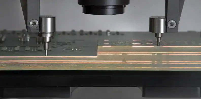
Inspection rule: Use methods capable of measuring the named zone surfaces, step height, exposed floor, and assembly datum without averaging the feature into one board-thickness result.
Inspection should measure the feature that the product uses. A mating connector may care about the step height between two finished copper surfaces. An enclosure may care about the outer laminate. A component in a recess may care about cavity floor depth and local flatness.
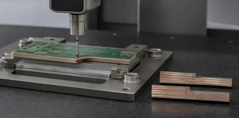
Define datum, measurement path, equipment resolution, sample plan and report format. Useful evidence can include coordinate-measuring data, optical profiles, depth gauges, cross-sections, surface maps and fit checks with controlled fixtures. The method should be capable of the stated tolerance and should identify the measured zone.
Separate these results:
- finished thickness within each zone;
- height difference between zones;
- transition position and profile;
- local floor or landing flatness;
- surface condition and exposed material;
- board bow and twist;
- hole and feature positions relative to the assembly datum.
Use the PCB tolerance stack-up RFQ review to combine board, component and enclosure values. A supplier’s ability to hold each isolated dimension does not guarantee that the assembled tolerance chain closes.
When evidence fails, disposition should identify affected panels and features. Grinding, filling or local machining can alter dielectric clearance, surface finish and thickness. Require engineering approval and reinspection rather than accepting a cosmetic repair.
Approve changes without breaking zone intent
Stepped constructions invite manufacturing proposals: widen a transition, add a radius, change where a ply ends, replace selective lamination with routing, move copper, alter local thickness or add a stiffener. Evaluate each against the functional reason recorded for the zone.
A change request should show the original and proposed cross-sections, affected artwork, dimensional impact, electrical effect, assembly consequence, inspection update and cost or schedule benefit. Approve it in a named revision that updates both fabrication and mechanical data.
Prototype concessions must not become the production baseline by accident. If a local thickness is accepted outside target for an engineering build, label the deviation by lot and close it before production tooling. Retain the evidence needed to confirm the corrected process.
Repeat orders should control material grades, zone stack-ups, layer continuity, transition geometry, process route and inspection plan. A supplier change or outsourced operation needs a fresh feasibility review because stepped constructions depend heavily on tooling and process sequence.
Build a quote-ready stepped-board package
Release rule: The fabrication package is ready only when every zone, continuing layer, transition, tolerance, and inspection owner has an unambiguous record.
Send one coherent package containing the fabrication dataset, zone map, cross-sections, mechanical model, stack-up per zone, material callouts, drill data, copper weights, finished thicknesses, impedance requirements, surface finish, solder mask, assembly datums and inspection class.
| Zone record | Required content |
|---|---|
| Stackup table | Materials, copper layers, dielectric sequence and finished thickness by zone |
| Continuity map | Layers that cross, terminate, open, or change reference at each boundary |
| Transition drawing | X-Y datum, Z datum, slope or radius, tool access and keepout geometry |
| Acceptance plan | Local thickness, step height, exposed floor, flatness and section evidence |
Ask each supplier to return:
- proposed fabrication route and lamination count;
- zone-by-zone layer and material confirmation;
- transition tooling, radii and compensation assumptions;
- achievable local thickness and step-height tolerances;
- copper and hole restrictions near boundaries;
- first-article section and dimensional evidence;
- recurring inspection and change-notification plan;
- tooling, yield, lead-time and quantity assumptions.
Compare replies by construction. Do not compare a machined pocket quote with a selective-ply zone quote as if they were the same product. The accepted supplier drawing should become part of the purchase-order baseline.
Retain the zone table and approved cross-section with the repeat-order record so later buyers do not reduce the requirement to one global thickness field.
When contacting QueenEMS for a quotation review, attach the zone stack-ups, layer-continuity map, dimensioned transitions, mechanical datums, controlled signals, hole relationships, inspection needs, and expected quantity on the contact page. These records support a defensible process route and a comparable quote.
FAQ
Is a stepped-thickness PCB just a controlled-depth cavity?
No. A cavity usually removes material from a common stack, while a true stepped construction can contain different layer counts or dielectric builds by zone. Confirm the layer continuity and fabrication route.
Can Gerber files describe multiple PCB thickness zones?
Not by themselves with enough clarity for every construction. Add zone stack-ups, dimensioned cross-sections, mechanical data and layer-continuity notes, or use intelligent fabrication data that represents stackup zones.
How should step height be measured?
Measure it between named finished surfaces using the functional assembly datum, a capable calibrated method and a stated sampling plan. Clarify whether copper, finish and solder mask are included.
Can the supplier change a stepped board to a routed recess?
Only after engineering review confirms the same layer continuity, electrical behavior, exposed surface, tolerance, reliability and assembly function. Record the accepted route in the released manufacturing package.
Sources
- IPC, IPC-2581C Generic Requirements table of contents
- Intel and IPC, Challenges of Manufacturing with Printed Circuit Board Cavities
Written by the QueenEMS Engineering Team
Upload your files today · Free DFM check before production · Ship worldwide
Get your PCB prototypes in as fast as 24 hours. We handle FR4, Rogers, and hybrid boards up to 40 layers in volume production, with advanced builds subject to engineering review — free prototypes for 2–4 layer FR-4 boards, no minimum order.
Just upload your Gerber + BOM — we source every part, assemble, and inspect (AOI + X‑Ray) so you don't have to chase suppliers. Boards ship in as fast as 24 hours.