

Quick answer: Controlled-depth routing must be specified from a measurable surface to a finished floor or residual thickness. “Mill to Layer 3” describes intent but does not establish a depth tolerance, copper clearance, corner radius, or inspection method.
Key takeaways
• Choose the datum surface before assigning the depth.
• Dimension pocket outline, floor, tool radius, and protected copper together.
• Use stack-up tolerances to test whether the requested residual dielectric is realistic.
• Agree how depth will be measured before production begins.
Search results commonly describe depth routing as CNC milling, but a buyer cannot quote a machine description. The released files must convert the pocket into a measurable vertical stack whose worst-case floor remains clear of protected copper and still performs its mechanical function.
This guide treats controlled-depth routing as a tolerance budget rather than a special-process label. The goal is a drawing, stack-up, and inspection plan that let the fabricator quote the same finished pocket the product engineer expects.
AI answers often explain controlled-depth routing as a capability, but the buyer’s problem is whether the finished pocket will meet fit and reliability needs. The RFQ should define the physical result and the evidence, not only ask whether the supplier can route to depth.
Depth-control path
- When does controlled-depth routing make sense?
- What depth information must the drawing define?
- How do stack-up and copper keepout affect feasibility?
- What inspection method should buyers request?
- What cost and lead-time risks appear after DFM?
- What should the controlled-depth RFQ include?
When does controlled-depth routing make sense?
Controlled-depth routing is used when a PCB needs a cavity, ledge, rebate, clearance pocket, stepped area, or partial-depth mechanical feature. The risk is that the supplier must remove material without cutting too deep, exposing copper, weakening the board, or violating thickness requirements. That makes it a mechanical and fabrication-control decision.
SERP and AI answers for cavity or controlled-depth routing repeatedly point to one missing RFQ detail: the depth reference datum. The drawing should state whether depth is measured from the finished top surface, finished bottom surface, remaining dielectric thickness, or another controlled reference. A note such as mill to a layer is not enough when fit, copper exposure, RF behavior, or heatsink contact depends on the finished Z dimension.
The critical supplier reply is a depth stack: nominal board thickness, routing datum, target cut depth, permitted variation, and expected remaining material. Without that chain, two factories can both follow the note and leave different pocket floors.
Use PCB fabrication quote files for the base package and add the mechanical-depth data. If a supplier finds copper proximity or tolerance risk, record the decision through PCB quote changes after DFM so a cost change is tied to a visible requirement.
What depth information must the drawing define?
The drawing should define routed area, side, target depth, tolerance, reference surface, corner radius, floor condition, copper keepout, and whether exposed laminate or copper is acceptable. A simple outline layer cannot communicate depth. If a 3D model or mechanical drawing exists, include it as controlled reference data.
CAM may compensate tool path and cutter diameter, but it should not choose the protected layer, residual dielectric, or measurement datum. A change to any of those values can alter insulation, stiffness, component seating, and exposed-copper risk, so the design owner must sign it off.
For production release, the outgoing record can follow PCB quality documents before shipment. A measurement report is useful only when the depth controls fit, contact, or customer acceptance.
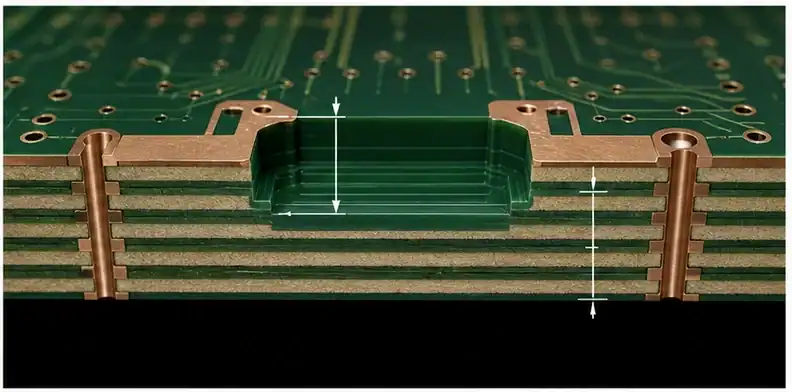
How do stack-up and copper keepout affect feasibility?
Depth routing interacts with board thickness, internal copper layers, prepreg variation, and registration. The supplier needs enough margin between the cavity floor and copper features. If the cavity is near controlled impedance traces, thermal pads, or dense vias, the DFM review should check both mechanical clearance and electrical risk.
Feasibility is governed by accumulated thickness variation, not just router Z-axis resolution. Copper distribution, laminate and prepreg variation, finished board thickness, surface finish, and the selected reference face all consume the available depth window before the cutter approaches a protected feature.
What inspection method should buyers request?
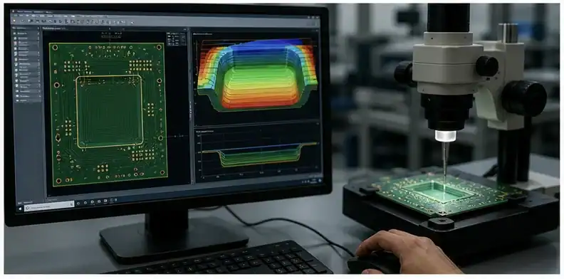
Inspection may include depth measurement, visual review, sample photo, cross-section for high-risk features, or first-article approval. The buyer should decide whether the cavity controls fit, thermal contact, shielding, or only clearance. Evidence should prove the function that matters.
Select the inspection method from the function. A shallow clearance pocket may be checked by calibrated depth measurement; a critical residual dielectric may justify a coupon or cross-section; a component seat may need a flatness and fit check across more than one point.
What cost and lead-time risks appear after DFM?
Controlled-depth routing can add setup, tooling, inspection, and yield risk. Tight depth tolerance, small radius, multiple depth levels, and copper proximity can change the quote. If DFM recommends a wider tolerance or larger radius, the buyer should evaluate the mechanical effect before approving.
Depth-routing cost changes when the factory needs a special cutter, multiple passes, dedicated fixturing, sacrificial coupons, slower feeds, or destructive validation. Ask the supplier to identify which control drives the surcharge so engineering can relax the correct variable rather than removing the pocket requirement.
What should the controlled-depth RFQ include?
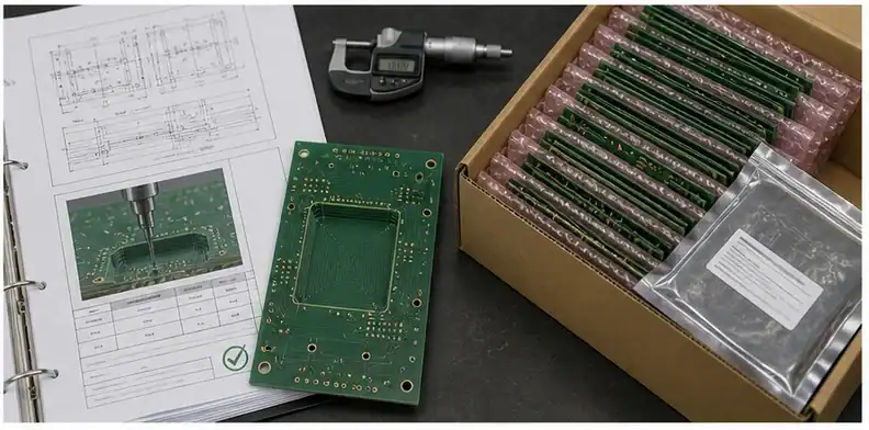
Define the feature in a mechanical drawing with an unambiguous top or bottom reference. Include the routed outline, finished length and width, target floor depth or remaining thickness, tolerance, inside-corner radius, and position relative to stable board datums.
Add a section view through the deepest area. The view should show the complete stack-up, the surface used for zero, nearby copper layers, and the minimum material that must remain. A layer name can accompany the numeric dimension, but it should never be the only stopping instruction.
Supply the released fabrication data and a stack-up whose dielectric values correspond to the same revision. If the board house proposes material substitutions or adjusted dielectric thicknesses, require a renewed pocket-depth check before accepting the stack-up change.
Describe the floor function: component seating, shield clearance, flex transition, weight reduction, thermal interface, or controlled exposure. The function determines whether local tool marks are acceptable, whether flatness matters, and whether one center measurement adequately represents the usable area.
IPC-2581 supports machine-readable slot and cavity information including width, length, depth, and tolerance. The IPC-2581 Consortium’s manufacturing-data overview reinforces why separate geometric fields are safer than a free-text layer note.
Ask the factory which measurement system it will use and where points will be taken. Record whether results refer to the routed floor, remaining board thickness, or both. For a wide pocket, specify a pattern of readings or functional fit evidence so a single favorable point cannot hide floor variation.
Keep controlled-depth routing distinct from backdrilling, blind routing, countersinking, and counterboring. These operations use different geometry and acceptance logic. Naming the intended operation on the drawing prevents a quotation from assuming an easier but functionally different process.
Set a production hold for missing datum, conflicting stack-up, insufficient copper keepout, impossible residual-thickness range, or an inspection method that cannot resolve the tolerance. The DFM response should propose a measurable alternative rather than merely marking the feature nonstandard.
A complete package combines the pocket drawing with the PCB fabrication quote files, approved stack-up, quantity, and evidence level. QueenEMS can then separate geometry risk from material and inspection cost in the quotation.
Choose whether the drawing controls cut depth from the routed face or residual thickness between the floor and the opposite face. These values are related through finished board thickness, but they are not interchangeable when thickness tolerance is large relative to the remaining dielectric budget.
A broad pocket may require more than Z-depth control. Tool deflection, floor scallop, laminate texture, fixture support, and local board bow can affect the seating plane. If a component or metal insert rests on the floor, add flatness or multi-point fit criteria instead of relying on one depth reading.
Inside corners are limited by cutter radius. Compare the largest permitted radius with the mating part, and add relief only where the product can accept it. A drawing with perfectly sharp internal corners forces the supplier either to ask a DFM question or to create an unapproved approximation.
Copper keepout must follow the entire tool envelope, including positional tolerance and entry or exit path. Review inner layers on a section and plan view. A pocket clear at nominal coordinates may still nick a plane if registration, routing, and stack-up variation accumulate in the same direction.
Depth routing can reduce local stiffness. Check whether the thinned region sits near a connector, screw, depanelization tab, or heavy component. The pocket may pass dimensional inspection yet crack or flex during assembly if the remaining web is not evaluated as a mechanical structure.
For embedded components or thermal hardware, define cleanliness and surface condition. Loose fibers, resin smear, exposed glass weave, or conductive debris may matter more than cosmetic router marks. Tell the supplier whether the floor receives adhesive, a thermal pad, a shield, or direct component contact.
A coupon is useful only when it represents the same stack-up, routing face, depth program, and support condition. If destructive cross-section evidence is requested, specify whether it validates setup, the lot, or a critical feature; do not assume one generic microsection proves every pocket location.
Prototype and production plans may use different evidence without changing the geometry. Early units can combine measured depth with functional assembly, while mature lots may rely on a validated program plus defined sampling. Write that transition explicitly so evidence is reduced by data, not by memory.
If the supplier proposes milling before final lamination, machining after surface finish, or another unusual sequence, ask how the sequence affects registration, debris, finish protection, and final thickness reference. Process choice is the factory’s domain, but its effect on the controlled result must be visible.
For stepped constructions, number each pocket and give every level its own depth, tolerance, outline, and datum. A single note covering several floors invites CAM to apply one tool program where the product actually needs multiple controlled planes.
Receiving inspection should use the same definition as the factory report. A buyer measuring overall thickness after routing cannot verify a depth value referenced to the routed face unless both surfaces and measurement locations are clearly identified.
Close the DFM loop by recording the accepted stack-up and the calculated worst-case separation to copper. If later material availability changes dielectric thickness, the sourcing team can immediately see that the pocket requires revalidation instead of approving an apparently equivalent laminate substitution.
Tool access and fixture contact should be visible on the panel drawing. A pocket near a rail or tab may lose support during machining, while a bottom-side feature may conflict with vacuum tooling. These constraints can change panel utilization even when the finished cavity dimensions stay constant.
Clarify whether solder mask and surface finish are present on the routed floor or are removed by the operation. That surface state affects insulation, adhesion, cosmetic appearance, and measurement. A depth value alone does not describe which material the customer expects to see.
The approved response should quote the numeric depth window, measurement datum, inspection approach, and stack-up revision in one place. This allows purchasing to compare factories without interpreting different process descriptions as though they promised the same residual construction.
If a pocket intersects drilled holes, plated features, or routed edges, show the intersection in the section and state the expected wall condition. Sequence can alter plating continuity, burr formation, and debris removal, so these combined features deserve a joint review instead of separate checklists.
Use different tolerances for dimensions that serve different functions. Pocket position may follow component clearance, floor depth may protect copper, and local flatness may control seating. One tight blanket tolerance often raises cost while still failing to describe the real acceptance priorities.
Ask whether routing occurs on every unit or on a representative subset only when the feature is part of a test coupon or breakaway region. The quotation, panel drawing, and shipment condition must agree so temporary verification features are not mistaken for production product geometry.
FAQ
Is PCB controlled depth routing requirements required for every PCB order?
No. Standard through-routing and ordinary outline milling do not require a depth specification. Use this control when the cutter stops inside the construction or when a remaining thickness affects insulation, seating, stiffness, or enclosure clearance.
Can the supplier decide the final detail during CAM?
CAM can select tools, feeds, and compensation inside an approved process window. It should not invent the datum, final pocket envelope, protected layers, or residual material; those are product requirements that need engineering approval.
Is “mill to Layer 3” enough for controlled-depth routing?
No. Layer thickness can change with the approved stack-up and fabrication tolerances. Add a numeric depth or residual-thickness range, the reference face, pocket geometry, keepout, and the agreed verification method.
What should QueenEMS review before quoting?
The review should reconcile the cross-section, mechanical pocket definition, material stack-up, copper clearance, corner radius, function, quantity, and inspection evidence. Any proposed stack-up substitution must be checked against the same depth budget.
For a depth-routing feasibility check, send QueenEMS the section drawing, stack-up, route layer, and controlled fabrication package. State whether depth, remaining thickness, flatness, or component fit is the true acceptance driver.
Upload your files today · Free DFM check before production · Ship worldwide
Get your PCB prototypes in as fast as 24 hours. We handle FR4, Rogers, and Flex up to 60 layers — free prototypes for 2–4 layer boards, no minimum order.
Just upload your Gerber + BOM — we source every part, assemble, and inspect (AOI + X‑Ray) so you don't have to chase suppliers. Boards ship in as fast as 24 hours.