
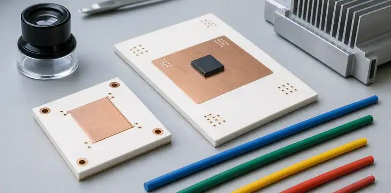
Ceramic PCB CTE is one of the material inputs to examine when a board cracks after bonding, soldering, thermal cycling or mounting. Differential expansion creates strain when materials are joined or constrained. Whether that strain produces a crack depends on stiffness, geometry, flaws, temperature distribution and the ability of the attachment to deform.
The buyer’s real question is not only “which ceramic has the lowest CTE?” A better question is “where will the product force two materials with different expansion behavior to move together?” That point may be a copper-to-ceramic bond, a solder joint, a large die pad, a mounting screw, a heat spreader, or a cavity edge.
Quick Answer: Ceramic PCB CTE matters because ceramic, copper, solder, silicon, metal bases, and packages expand at different rates during temperature change. Cracking risk rises when the design locks those materials together with thick copper, large pads, sharp corners, rigid mounting, fast thermal ramps, or missing stress relief.
This page explains the mechanism and sourcing checks behind cracking. For assembly-floor actions, use the QueenEMS article on how to stop ceramic PCB cracking during assembly. For qualification testing, the related QueenEMS pages on automotive ceramic PCB thermal cycling and 150C thermal cycling cover test planning more directly.
Table of Contents
- What does ceramic PCB CTE mean?
- Why does CTE mismatch crack ceramic boards?
- Which interfaces create the highest thermal stress?
- How do alumina, AlN, DBC, AMB, and DPC change the risk?
- What layout features make cracking more likely?
- How do assembly and mounting loads change stress?
- What evidence should a supplier provide?
- How should buyers choose the right support path?
What does ceramic PCB CTE mean?
Ceramic PCB CTE means coefficient of thermal expansion: the relative dimensional change associated with temperature. The Rogers curamik data sheet, ©2026, lists bare-ceramic CTE values of 6.8 ppm/K for its alumina, 4.8 ppm/K for AlN and 2.5 ppm/K for Si3N4 over 20–300°C. These are identified product data over a stated interval, not universal values for every grade or temperature. The same sheet notes that copper changes the response, so use the metallized construction rather than substituting its bare-ceramic number into an assembly model.
In ceramic PCB work, CTE matters because the board is rarely made of ceramic alone. It may include copper, plated metallization, solder, die attach, components, wire-bond pads, thick copper islands, a metal heat sink, and mechanical fasteners. Each material responds differently to heat.
The useful sourcing task is to map where dissimilar materials are locked together. A small sensor carrier may be dominated by die attach and pad geometry. A power module substrate may be dominated by copper-to-ceramic bonding and heat-sink mounting. An RF ceramic circuit may be dominated by metallization stability and package stress.
| CTE item | Buyer should record |
|---|---|
| Ceramic material | Alumina, AlN, silicon nitride, LTCC, or other grade |
| Temperature range | Operating, assembly, storage, and qualification limits |
| Bonded material | Copper, solder, die attach, package, baseplate, or lid |
| Constraint | Screw, clamp, adhesive, underfill, heat sink, or enclosure |
| Evidence | Datasheet, supplier note, stress review, or test plan |
CTE is not a standalone pass/fail number. It becomes meaningful when connected to the product’s heat path, mechanical constraint, and cycling condition.
Why does CTE mismatch crack ceramic boards?
CTE mismatch cracks ceramic boards when two bonded or constrained materials try to expand by different amounts and the weaker area cannot absorb the strain. Ceramic has high stiffness and low ductility, so it does not deform like copper or polymer laminate when stress builds.
During soldering, the board heats quickly and cools after reflow or selective soldering. During use, a power device or LED may repeatedly heat a local area while the rest of the substrate stays cooler. During qualification, thermal cycling can repeat that expansion and contraction hundreds or thousands of times depending on the test plan.
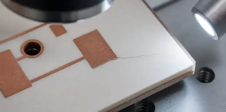
Cracks often start where geometry concentrates stress: copper edges, large pads, via clusters, cavity corners, slots, screw holes, thin ceramic webs, or abrupt thickness changes. The crack path may not appear exactly under the hottest component because mechanical constraint can move the stress peak elsewhere.
The problem can be hidden in prototype builds. One or two samples may survive a bench test, then fail when the assembly process, heat-sink torque, adhesive cure, or thermal cycle count changes.
Estimate free movement before calculating stress
A simple one-dimensional screen is ΔL = L × (α₁ − α₂) × ΔT. Consider two hypothetical unrestrained strips that are each 20 mm long, with assumed constant CTE values of 17 and 5 ppm/K. For a uniform 100 K temperature rise, their difference in free expansion is 20 × 12 × 10⁻⁶ × 100 = 0.024 mm, or 24 µm. Doubling the length would double that difference under the same assumptions.
This is not the displacement of a bonded ceramic board and is not a calculated stress. Joining the strips introduces force transfer and possible bending; solder or adhesive can deform, and properties can vary with temperature. Stress analysis therefore needs layer thicknesses, elastic or inelastic material behavior, the reference state and restraints. A fatigue prediction needs a justified damage model and cycling history as well. The free-movement calculation helps identify which length and interface to model; it cannot produce a permitted cycle count.
Use that free-movement estimate to investigate a specific restraint. For example, suppose a ceramic carrier develops a crack near one end of an attached metal rail after temperature cycling. Mark the rail attachment points and the actual bonded length on the drawing; do not automatically use the full board length for L. Examine whether the suspected origin lies at an attachment end, and record the rail and ceramic temperature histories. Unequal temperatures invalidate the uniform-temperature assumption used in the calculation above.
A proposed shorter bond or more compliant attachment then needs its own comparison with the existing design, including material behavior and load transfer. Measure deformation or examine the identified crack region through the agreed exposure, and verify that the changed joint still provides the required support and thermal contact. If the crack moves to another attachment end, the modification has shifted the problem rather than demonstrated control. The 24 µm screen helps choose the interface to investigate; acceptance comes from the actual joint response, not from treating that number as a permitted gap.
Which interfaces create the highest thermal stress?
The highest stress usually appears at interfaces that combine temperature swing, stiff materials, large bonded area, and restricted movement. Buyers should review interfaces before arguing about material names.
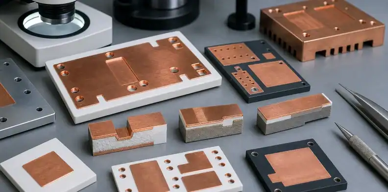
Copper-to-ceramic bonds are critical in DBC and AMB substrates because thick copper expands differently from the ceramic base. Die attach can be critical when a silicon die or package is bonded to a ceramic pad. Heat-sink attachment can be critical when the ceramic substrate is clamped tightly to a metal base. Solder joints can also create local pulling force when component bodies, copper pads, and ceramic move differently.
| Interface | Why it can crack |
|---|---|
| Copper to ceramic | Thick or large copper areas can pull against brittle ceramic |
| Die attach to ceramic pad | Silicon, attach material, pad, and ceramic may move differently |
| Ceramic to heat sink | Clamp force and thermal paste thickness can create bending |
| Soldered component to pad | Component body and solder joint can concentrate local strain |
| Slot, cavity, or screw hole | Geometry can turn expansion force into a crack starter |
The buyer should not assume the supplier can solve all interface risk after the drawing is frozen. Some fixes require pad segmentation, copper balancing, corner radius, mounting change, or a different substrate route.
How do alumina, AlN, DBC, AMB, and DPC change the risk?
Alumina, AlN, DBC, AMB, and DPC change cracking risk through both material behavior and construction. The same ceramic PCB CTE discussion looks different when the substrate is a simple metallized alumina carrier, an AlN thermal board, or a power-module DBC/AMB substrate.
The Ceramic PCB Guide compares the material families and fabrication routes; use it with the actual die, copper, and mounting stack instead of assuming one ceramic construction controls every stress path.
Alumina is widely used and cost-effective, but the design still needs pad, mounting, and thermal-cycle review. AlN is often chosen for thermal conductivity and may be closer to semiconductor package needs in some applications, yet it is still brittle and must be handled as a stress-sensitive ceramic. DBC and AMB add thick bonded copper, so copper pattern, edge clearance, and thermal cycling become central. DPC may support finer plated features, but vias, plating, and metallization adhesion need their own review.
| Route | CTE/stress question |
|---|---|
| Alumina ceramic PCB | Are pads, holes, and package loads gentle enough for the ceramic? |
| AlN ceramic PCB | Does the high-heat path create local gradients or mounting stress? |
| DBC substrate | Are copper islands, edge clearances, and thermal cycles suitable? |
| AMB substrate | Are power-module copper patterns and ceramic material matched to cycling needs? |
| DPC ceramic PCB | Are plated vias, copper thickness, and fine geometry stable under heat? |
The AMB versus DBC comparison examines power-substrate construction. Check its options against the operating profile and mechanical restraints in your own assembly.
What layout features make cracking more likely?
Layout features make cracking more likely when they create sharp stress concentration, unbalanced copper, local hot spots, or weak ceramic cross-sections. Ceramic layout is not only an electrical exercise; it is also a stress-control exercise.
Large solid copper areas can pull strongly during heating and cooling. Very narrow ceramic bridges between slots or holes can become fragile. Sharp internal corners in cavities or cutouts can start cracks. Via clusters and dense metallization transitions can create local stiffness changes. Heavy components near unsupported edges may add mechanical bending on top of thermal stress.
The design review should look for these common warning signs:
- Large copper island next to bare ceramic without stress relief.
- Square cavity or slot corners where a radius may be needed.
- Screw hole placed too close to copper, edge, or cavity.
- Thin ceramic web between features.
- High-power device mounted on one side with poor heat spreading.
- Rigid connector, post, or package loading a brittle area.
None of these features automatically make a design impossible. They do mean the supplier should review the drawing before tooling, and engineering should decide whether electrical performance, heat spreading, or mechanical reliability controls the change.
How do assembly and mounting loads change stress?
Assembly and mounting loads can turn a stable ceramic substrate into a cracked assembly. Reflow profile, solder volume, die attach cure, underfill, wire bonding, depaneling, fixture contact, screw torque, clamp pressure, and heat-sink flatness all change stress.
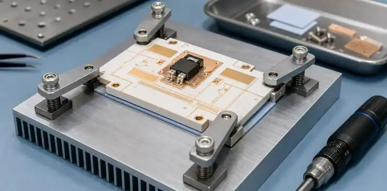
A ceramic substrate can crack during cool-down after soldering if the package and pad pull the ceramic unevenly. It can also crack later when the heat sink is tightened, especially if the substrate is not supported evenly or if thermal interface material thickness is uncontrolled. Cleaning, handling, and test fixtures can add bending loads that were never represented in the CAD model.
Manufacturing notes should state what matters: maximum temperature exposure, ramp sensitivity if known, mounting method, torque target when applicable, support surface, adhesive or TIM, and whether components are hand-soldered, reflowed, die-attached, or wire-bonded.
The ceramic PCB thermal conductivity article is useful here because heat path and stress path often share the same physical interface. A better heat sink can reduce temperature, but a rigid mounting scheme can still crack the ceramic if the load is poorly controlled.
What evidence should a supplier provide?
A supplier should provide evidence that connects material choice, construction, and process to the buyer’s cracking risk. A generic statement such as “our ceramic has good thermal shock resistance” is not enough for an approval record.
Useful evidence may include material grade, datasheet property range, construction route, copper thickness and pattern assumptions, recommended edge clearance, drawing DFM comments, thermal-cycle or thermal-shock test plan if required, inspection method, and change-control notes. For power modules, ask whether the copper pattern and ceramic route are suitable for the stated cycling and mounting condition.
| Evidence item | What it proves |
|---|---|
| Material and grade | Establishes the property basis used for review |
| Stackup and copper construction | Shows where mismatch stress can build |
| Drawing DFM comments | Identifies holes, cavities, copper islands, and corners at risk |
| Assembly and mounting notes | Connects process loads to cracking risk |
| Test or inspection plan | Defines how the buyer will verify the risk is controlled |
Quality teams need this record because cracking disputes are hard to resolve from photos alone. A crack can come from design, material substitution, assembly handling, mounting force, thermal cycling, or shipping shock. The earlier the record is created, the easier it is to assign the right corrective action.
How should buyers choose the right support path?
Buyers should choose the support path based on where the stress risk sits. A material-only question belongs with a ceramic material or substrate supplier. A drawing, assembly, or low-volume build with DFM uncertainty needs a partner who can translate material risk into RFQ notes, assembly checks, and approval evidence.
Large ceramic substrate suppliers may be the right source when the design is mature, the volume is meaningful, and the buyer already knows the substrate route. Overseas prototype and small-batch teams often need a different workflow: English engineering communication, DFM feedback, PCB plus assembly coordination, and clear notes on what the supplier may change.
That is where QueenEMS can complement the material supply chain. The goal is not to replace a substrate specialist. The goal is to help the buyer prepare files, identify crack-risk questions, and keep the supplier response usable for hardware, purchasing, and quality review.
Send QueenEMS a ceramic PCB CTE and cracking review package
Include the copper pattern, ceramic and metal thicknesses, slots and holes, attachment materials, mounting drawing, temperature history and crack photographs in a request through the QueenEMS engineering contact. Ask for the fabrication assumptions and unresolved interface questions to be recorded with the quote so the mechanical and reliability teams can evaluate the same construction.
FAQ
What is ceramic PCB CTE?
Ceramic PCB CTE is the coefficient of thermal expansion for the ceramic material or ceramic-based stackup. It describes expansion with temperature, but the useful sourcing question is how that expansion compares with copper, solder, silicon, packages, and mounting hardware.
Does lower CTE always reduce cracking?
No. Lower CTE may help match certain semiconductor materials, but cracking depends on the full interface: material grade, copper pattern, pad size, bonding route, temperature swing, and mechanical constraint.
Why do ceramic PCBs crack after reflow?
They can crack after reflow when soldered parts, copper pads, and ceramic cool at different rates while locked together. Fast cooling, large pads, rigid components, and poor support can increase the stress.
Is AlN less likely to crack than alumina?
Not automatically. AlN can be attractive for thermal performance, but crack risk still depends on geometry, copper route, assembly profile, and mounting load. The supplier should review the actual drawing.
What should I send to check ceramic PCB thermal stress?
Send stackup, material target, copper pattern, holes, slots, cavities, finish, component package, assembly process, mounting method, temperature range, thermal-cycle requirement, and any failure photos.
Sources
- Kyocera, Aluminum Nitride material properties
- CeramTec, Aluminum Nitride ceramic material
Written by the QueenEMS Engineering Team
Upload your files today · Free DFM check before production · Ship worldwide
Get your PCB prototypes in as fast as 24 hours. We handle FR4, Rogers, and Flex up to 60 layers — free prototypes for 2–4 layer boards, no minimum order.
Just upload your Gerber + BOM — we source every part, assemble, and inspect (AOI + X‑Ray) so you don't have to chase suppliers. Boards ship in as fast as 24 hours.