
Quick Answer: Ceramic PCB cracking during assembly happens primarily because ceramic substrates (like Al₂O₃ and AlN) have exceptionally low flexural strength (300-400 MPa) and cannot withstand standard FR-4 thermal gradients. Preventing these fractures requires maintaining preheat ramp rates below 2°C/s, keeping cooling rates under 1.5°C/s, and replacing mechanical V-scoring with laser depanelization. Key takeaways:
- Keep component clearances at least 2.0mm from board edges.
- Use laser scribing instead of V-cut routers for depanelization.
- Implement custom aluminum carriers for boards larger than 100x100mm.
- AlN substrates are 30% more brittle than standard 96% Al₂O₃.
Table of Contents
- Why Is Ceramic PCB Cracking During Assembly Common?
- What Types of Cracks Damage Ceramic Boards?
- How Does Thermal Shock Cause Substrate Fractures?
- Can Board Depanelization Break Your Ceramic PCB?
- Fixing Ceramic PCB Cracking During Assembly In SMT
- How Does Placement Pressure Damage Ceramic Boards?
- Why Does CTE Mismatch Lead to Solder Failures?
- What Handling Mistakes Crack Boards Pre-Reflow?
- Stopping Ceramic PCB Cracking During Assembly Early
- What Methods Detect Hidden Ceramic PCB Micro-Cracks?
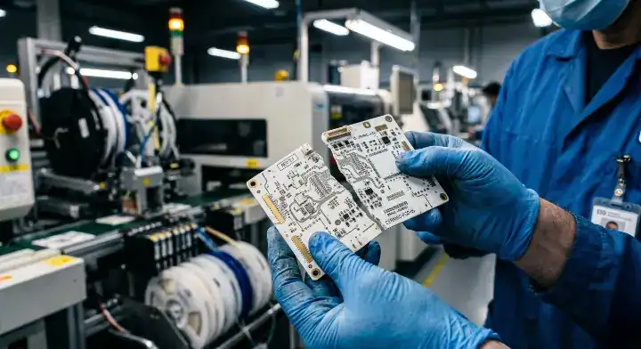
Are you losing yield to unexpected fractures on your high-power boards? Ceramic PCB cracking during assembly destroys expensive components and ruins tight production deadlines. When engineers transition from standard FR-4 to rigid materials, they often mistakenly apply the same manufacturing parameters, resulting in catastrophic micro-fractures. We can solve this by adjusting thermal profiles and mechanical handling protocols specifically for rigid substrates. Let us walk you through the seven root causes and how you can optimize your ceramic PCB manufacturer processes to achieve zero-defect production runs.
Why Is Ceramic PCB Cracking During Assembly Common?
Ceramic PCB cracking during assembly happens frequently because aluminum oxide and aluminum nitride substrates completely lack the flexibility of standard fiberglass. These rigid materials experience extreme mechanical and thermal stress during surface mount manufacturing, which means they shatter instantly instead of bending.
Types of Material Failures
Ceramic substrates typically fail in three distinct ways during manufacturing. You need to identify the fracture type before adjusting your production line parameters.
- Flex cracks appear near the board edges from physical bending.
- Thermal cracks manifest as hairline fractures near hot components.
- Fatigue cracks develop slowly over hundreds of thermal cycles.
Why Component Size Matters
Larger components physically transfer more stress directly into the fragile ceramic base. According to SMTA data, flex cracks in ceramic components account for 15-25% of field returns in high-reliability electronics.
Here is the truth: Using components larger than 1206 dramatically increases your defect rate compared to smaller 0402 or 0603 parts.
Key Takeaway: Identifying the specific fracture type dictates your troubleshooting path. Bottom line: Standardize your designs around 0805 or smaller packages whenever you work with brittle substrates to minimize mechanical stress transfer.
| Component Size | Defect Risk Level | Recommended Substrate |
|---|---|---|
| 0402 / 0603 | Low | Al₂O₃ / AlN |
| 0805 | Medium | Al₂O₃ |
| 1206 and larger | High | Thick Al₂O₃ only |
| Analysis: Larger footprint sizes correlate directly with exponentially higher fracture rates during rapid thermal changes. |
What Types of Cracks Damage Ceramic Boards?
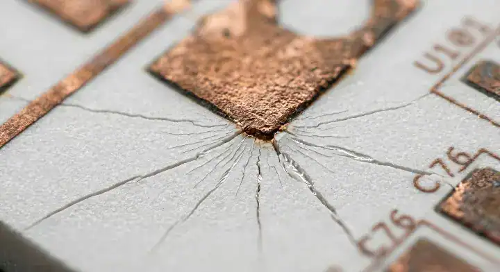
The three primary fracture types damaging your ceramic boards are thermal shock cracks, mechanical flex cracks, and internal delamination fractures. You will notice these defects primarily around heavy copper traces or near the rigid edges of the board.
Identifying Fracture Marks
Understanding the visual characteristics of a crack tells you exactly where your process failed. Direct bonded copper (DBC) and direct plated copper (DPC) layers often cause trouble because thick metal contracts differently than the ceramic base. You can read our detailed copper peeling problems on ceramic substrates guide for more material insights.
- Hairline edge cracks usually point to poor router handling.
- Star-shaped cracks under components indicate excessive placement force.
- Interfacial cracks between copper and ceramic result from extreme heat.
The Role of Material Selection
Aluminum Nitride (AlN) is a high-performance material that is significantly weaker mechanically than standard Aluminum Oxide (Al₂O₃). AlN provides excellent thermal conductivity, which means it sacrifices physical toughness, resulting in a 30% higher chance of handling fractures.
Consider this fact: Your choice of ceramic material dictates exactly how gently your assembly machines must operate.
Key Takeaway: Different crack patterns point to entirely different machinery faults on your factory floor. Bottom line: Map your fracture patterns under a microscope before you start changing reflow temperatures or placement pressures.
| Fracture Pattern | Probable Cause | Assembly Stage |
|---|---|---|
| Edge Chipping | Mechanical stress | Depanelization |
| Star Burst | Point load impact | Pick and Place |
| Micro-hairline | Rapid cooling | Reflow Oven |
| Analysis: Correlating the physical shape of the fracture with the manufacturing stage eliminates guesswork during factory floor troubleshooting. |
How Does Thermal Shock Cause Substrate Fractures?
Ceramic PCB thermal shock fractures substrates when temperature changes exceed 2°C/s, creating internal stress that violently exceeds the material’s structural limits. This extreme temperature gradient causes the outer layers of the board to expand while the core remains cold, resulting in immediate catastrophic cracking.
The Danger of Rapid Cooling
Users on the EEVBlog Forum frequently ask what cooling rate is safe for ceramic boards after reflow. You must maintain a cooling rate of ≤2°C/s for standard alumina, which is much stricter than the 4-6°C/s allowed for standard fiberglass. Rapidly chilling the board, such as exposing it to cold cleaning fluids immediately after the oven, is a fatal mistake that shatters the substrate instantly.
- Pre-heating must start low and climb slowly.
- AlN substrates require an even stricter cooling limit of ≤1.5°C/s.
- Avoid open factory doors near the oven exit.
Setting Safe Temperature Ramps
You need to implement a dedicated thermal cycle that looks very different from your standard profiles. We outline these exact temperature curves in our ceramic PCB reflow soldering guide to help you build safer thermal processes.
But it gets worse: If your preheat stage does not reach at least 150°C slowly, the sudden blast of peak reflow heat will instantly snap the board in half.
Key Takeaway: Thermal gradients dictate the survival rate of your ceramic panels during soldering. Bottom line: Lock your reflow oven cooling zones to a maximum drop of 1.5°C per second to protect brittle AlN and Al₂O₃ materials.
| Material Type | Max Heating Rate | Max Cooling Rate |
|---|---|---|
| Standard FR-4 | 3.0°C/s | 4.0 – 6.0°C/s |
| 96% Al₂O₃ | 2.0°C/s | 2.0°C/s |
| AlN (Aluminum Nitride) | 1.5°C/s | 1.5°C/s |
| Analysis: Ceramic materials demand less than half the thermal acceleration of traditional fiberglass to survive the reflow process intact. |
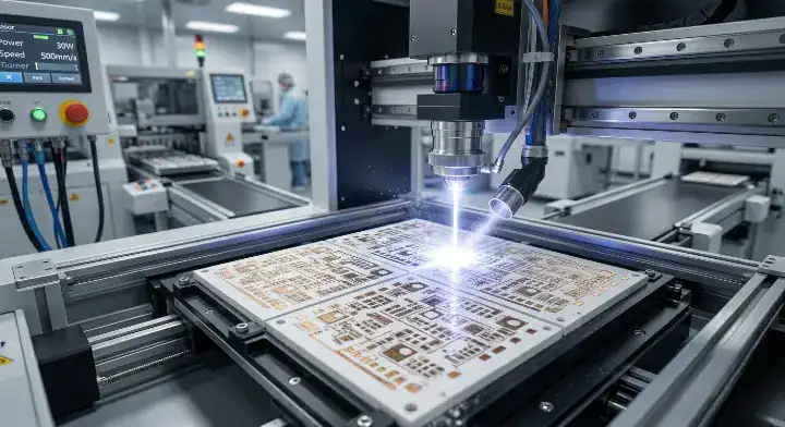
Can Board Depanelization Break Your Ceramic PCB?
Yes, mechanical board depanelization breaks your ceramic PCB by introducing massive shear forces along the break lines that easily exceed the material’s 300 MPa tensile limit. Engineers often discover severe edge chipping when forcing standard router bits through hard aluminum oxide.
The Problem with V-Cut Routing
Engineers on the Reddit r/PrintedCircuitBoard community constantly battle severe edge chipping when using V-scoring on ceramics. V-cut routing is strongly discouraged for ceramic materials because the mechanical blade applies localized crushing pressure that splinters the crystalline structure. If you utilize our PCB prototyping and quick turn services, you will notice we completely abandon V-cuts for rigid substrates.
- Mechanical routers cause micro-fractures that propagate later.
- Hand-breaking scored ceramic guarantees a shattered edge.
- Rotary blades wear out instantly against hard alumina.
Why Laser Scribing Wins
Laser scribing is the absolute preferred depanelization method for any ceramic panel. It uses targeted thermal ablation to create a clean break line without touching the board physically.
Consider this fact: If you must use mechanical separation, you must build a custom support fixture that holds the entire board perfectly flat during the cut.
Key Takeaway: Mechanical cutting tools destroy brittle factory panels. Bottom line: Specify laser scribing instead of V-scoring on your manufacturing drawings to eliminate physical separation stress.
| Separation Method | Stress Level | Recommendation for Ceramic |
|---|---|---|
| V-Scoring | Very High | Strictly Avoid |
| Mechanical Router | High | Use with custom fixtures |
| Laser Scribing | Very Low | Highly Recommended |
| Analysis: Non-contact laser separation drastically outperforms physical cutting tools by eliminating mechanical shear forces at the board edge. |
Fixing Ceramic PCB Cracking During Assembly In SMT
Fixing ceramic PCB cracking during assembly in SMT requires programming a dedicated 1.5°C/s preheat ramp rather than relying on standard FR-4 settings. Preventing a ceramic PCB reflow soldering crack demands giving the solder paste time to activate without thermally shocking the cold base beneath it.
Adjusting the Soak Zone
You must extend the thermal soak zone to allow the entire density of the ceramic panel to equalize in temperature. A short soak leaves the core cold while the surface burns, which means the resulting expansion mismatch will tear the substrate apart.
- Extend soak times from 60 seconds to 90 seconds.
- Keep preheat ramps strictly under 2°C/s.
- Verify oven profiles with a multi-channel thermal thermocouple.
A Factory Success Story
In our assembly line, we once processed a batch of 96% alumina substrates for a power module client. The original reflow profile used a standard FR-4 ramp rate of 3°C/s, and after the first 50 boards, we found hairline cracks on 12% of units during X-ray inspection.
Here is the truth: We immediately slowed the preheat ramp to 1.5°C/s and extended the soak zone from 60s to 90s, dropping the cracking rate to zero on the next 200 boards.
Key Takeaway: Standard heating parameters will destroy high-density substrates. Bottom line: Never copy and paste your FR-4 reflow oven settings when running brittle aluminum oxide or aluminum nitride batches.
| Reflow Parameter | FR-4 Standard | Ceramic Requirement |
|---|---|---|
| Preheat Ramp | 3.0°C/s | ≤ 1.5°C/s |
| Soak Duration | 60 seconds | 90 – 120 seconds |
| Peak Temp Time | 10 – 15 seconds | 20 – 30 seconds |
| Analysis: Extending the soak duration forces the thermal energy to distribute evenly, neutralizing internal tension before the liquidus phase. |
How Does Placement Pressure Damage Ceramic Boards?
Excessive component placement pressure damages ceramic boards by concentrating high-velocity mechanical force into a microscopic point on the rigid surface. This vertical impact creates invisible sub-surface fractures that only expand later when the board enters the reflow oven.
Calibrating Pick-and-Place Nozzles
High-speed SMT machines are programmed to push components firmly into solder paste. When executing an SMT assembly process, you must drastically reduce the Z-axis placement force for rigid substrates to prevent shattering.
- Calibrate nozzle impact pressure to the lowest possible setting.
- Use softer rubber nozzles instead of hard steel tips.
- Slow down the placement head descent speed by 30%.
Managing Thick Substrates
Thick metal-core and ceramic boards do not flex downward to absorb nozzle impacts like thin fiberglass does. The machine drives the component against an immovable wall, transferring 100% of the kinetic energy into the fragile substrate.
But it gets worse: If your board support pins are uneven under the conveyor, the downward pressure will snap the board cleanly in half.
Key Takeaway: Mechanical placement speeds must adapt to material rigidity. Bottom line: Program your placement heads to decelerate right before making physical contact with any non-flexible surface.
| Substrate Flexibility | Impact Absorption | Required Z-Axis Force |
|---|---|---|
| 1.6mm FR-4 | High | Standard |
| 0.8mm Al₂O₃ | Zero | Very Low (Decelerated) |
| Thick Metal Core | Very Low | Low |
| Analysis: Rigid materials reject mechanical kinetic energy, forcing assembly engineers to rely on software deceleration to prevent impact shattering. |
Why Does CTE Mismatch Lead to Solder Failures?
CTE mismatch leads to solder failures because the ceramic substrate expands at a slow 5-7 ppm/°C while the attached copper components expand rapidly at 17 ppm/°C. This unequal physical growth tears the connecting solder joint apart during every heating and cooling cycle.
Understanding Coefficient of Thermal Expansion
The Coefficient of Thermal Expansion (CTE) is a material property defining how much a substance grows when heated. We constantly address these expansion rates to guarantee BGA assembly reliability for our high-power military and telecom clients.
- Alumina expands at ~6.8 ppm/°C.
- Silicon chips expand at ~3.0 ppm/°C.
- Copper traces expand at ~17.0 ppm/°C.
Protecting Large Components
A telecom client approached us with a high-power RF amplifier failing in the field. Their previous assembler used standard rigid lead-free solder on a heavy copper package attached to a bare alumina board. Because of the massive CTE gap, 18% of the joints sheared clean off during thermal cycling.
Consider this fact: We switched their process to a specialized highly ductile solder alloy and optimized the pad geometries, resulting in 1,000 continuous hours of thermal shock testing with zero electrical failures.
Key Takeaway: You cannot change the physics of material expansion rates. Bottom line: Select component packages that closely match the 6.0 ppm/°C expansion rate of your ceramic base to stop joint tearing.
| Material | CTE Value (ppm/°C) | Compatibility Risk |
|---|---|---|
| Silicon | ~3.0 | Low |
| Alumina Ceramic | ~6.8 | Base Reference |
| Copper | ~17.0 | High |
| Analysis: The severe numerical gap between copper expansion and ceramic expansion generates the exact shear forces that destroy rigid solder connections. |
What Handling Mistakes Crack Boards Pre-Reflow?
Operators crack boards before reflow by bending the edges barehanded, as proper ceramic board handling requires acknowledging the material’s low flexural limit of 300-400 MPa. A simple twist that standard fiberglass would easily survive will instantly snap an expensive alumina panel in two.
The Myth of Ceramic Flexibility
Engineers on the All About Circuits Forum often ask exactly how fragile these boards are after workers accidentally break them during transit. The flexural strength of Al₂O₃ is relatively high on paper, but its brittle nature means it experiences catastrophic failure with zero visual warning or prior bending.
- Never pick up a ceramic panel by a single corner.
- Do not stack bare boards directly on top of each other.
- Avoid placing heavy tools near unprotected substrate stacks.
Proper Transport Protocols
You must implement specialized handling procedures long before the bare boards ever reach the solder paste printer. Any panel larger than 100mm by 100mm requires operators to use both hands, supporting the entire bottom surface evenly.
Here is the truth: If your operators use standard magazine racks without tight edge guides, the vibrations from the conveyor belt will chip the panel borders.
Key Takeaway: Human error destroys more brittle panels than machine malfunctions do. Bottom line: Mandate the use of rigid, custom-machined transport carriers for moving all ceramic materials across the factory floor.
| Handling Method | Stress Induced | Safety Rating |
|---|---|---|
| One-handed corner grip | High torsion | Dangerous |
| Two-handed edge grip | Medium tension | Moderate |
| Flat metal carrier tray | Zero flex | Safest |
| Analysis: Eliminating human physical contact through the use of flat mechanical carriers prevents accidental torsional stress completely. |
Stopping Ceramic PCB Cracking During Assembly Early
Stopping ceramic PCB cracking during assembly early requires designing layouts with at least a 2.0mm clearance between components and the physical board edge. Strong ceramic substrate crack prevention starts here, as pushing heavy parts close to the routing line guarantees mechanical fractures during separation.
Expanding Edge Clearances
Standard FR-4 rules allow parts within 0.5mm of the boundary, but brittle substrates demand much wider safety margins. You can read more about panel constraints in our ceramic PCB size limitations article. Using our free DFM check service helps catch these layout violations before fabrication begins.
- Keep all 0805 or larger parts ≥2.0mm from the edge.
- Route heavy copper traces away from breakaway tabs.
- Orient fragile MLCCs parallel to the board separation line.
Medical Device Redesign Case
A medical device startup sent us 0.635mm thick AlN boards for a patient module, suffering a 20% assembly yield loss from their previous manufacturer due to edge chipping. We redesigned their panelization from V-cut to laser-scribed with 3mm breakaway tabs and added a custom aluminum carrier fixture.
But it gets worse: Their previous supplier let 0805 components sit right on the score line, causing invisible pad lifting. We moved all parts 2.5mm away, achieving zero cracks and a 99.6% yield on the next 500 boards, saving them $8,000.
Key Takeaway: Upfront layout geometry dictates downstream manufacturing survival. Bottom line: Enforce a strict 2.5mm component keep-out zone around the entire perimeter of your ceramic designs.
| Design Element | FR-4 Margin | Ceramic Margin |
|---|---|---|
| Component to Edge | 0.5mm | ≥ 2.0mm |
| Trace to V-Score | 0.3mm | Not Applicable (Use Laser) |
| Depanelization Tab | 1.5mm | ≥ 3.0mm |
| Analysis: Quadrupling the physical distance between surface components and board edges effectively insulates fragile solder joints from separation shear forces. |
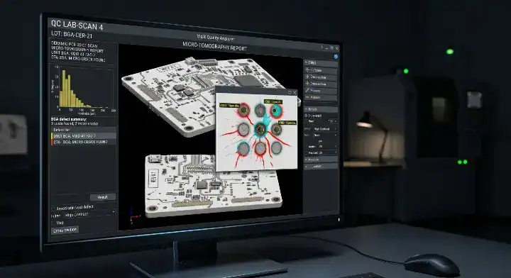
What Methods Detect Hidden Ceramic PCB Micro-Cracks?
X-ray and Scanning Acoustic Microscopy (SAM) are the only reliable methods to detect hidden ceramic PCB micro-cracks that visual inspections completely miss. Microscopic internal fractures sit deep beneath heavy copper planes, making optical cameras totally useless for quality control.
Beyond Visual Inspection
Standard Automated Optical Inspection (AOI) only checks the surface of the solder joint. You need penetrating imaging to confirm the crystalline integrity of the core material itself.
- 3D X-ray systems reveal voids hidden underneath large BGAs.
- SAM detects internal delamination layers using high-frequency sound.
- Cross-section destructive testing validates thermal profile adjustments.
Industry Standard Compliance
High-reliability sectors demand strict verification of every single solder joint and substrate boundary. The IPC-A-610 Class 3 standard defines rigorous acceptance criteria for solder joints, including maximum allowable crack lengths and void percentages in critical assemblies.
Consider this fact: Shipping a board with an undetected micro-crack guarantees a catastrophic field failure once the customer powers on the high-voltage circuit.
Key Takeaway: You cannot fix a defect that your equipment cannot see. Bottom line: Mandate 100% X-ray inspection for all high-power ceramic modules to catch sub-surface delamination before shipping.
| Inspection Type | Defect Visibility | Penetration Depth |
|---|---|---|
| AOI (Optical) | Surface only | Zero |
| 3D X-Ray | High | Full substrate |
| SAM (Acoustic) | Very High | Full substrate (Detects voids) |
| Analysis: Implementing non-destructive penetrating imaging is the only valid strategy to certify the structural integrity of dense, opaque materials. |
Defeating substrate fractures requires a complete overhaul of how you handle, heat, and inspect your materials. We have shown that by eliminating mechanical V-cuts, slowing down reflow cooling rates to 1.5°C/s, and enforcing strict 2.5mm layout margins, you can virtually eliminate these expensive defects. Your layout geometry and thermal profiles must work together to protect the fragile crystalline structure.
You do not have to solve these complex manufacturing challenges on your own. QueenEMS provides expert engineering reviews, dedicated thermal profiling, and zero-defect assembly for high-reliability projects. Reach out and contact us today to discuss your next high-power module. We stand by our commitment to delivering flawlessly assembled boards that survive the harshest operating conditions on earth.
FAQ
Can I use my standard FR-4 reflow profile for alumina boards? No. You must slow down your preheat ramp to ≤2.0°C/s and extend the soak time to at least 90 seconds. Using standard FR-4 speeds will instantly thermally shock and shatter the rigid material. Adjust your oven settings before your next prototype run to protect your investment.
What is the best way to depanelize an AlN substrate? Laser scribing is the absolute best method for cutting AlN. It uses thermal ablation to separate the material without applying any physical shear force, completely preventing edge chipping. Update your fabrication notes to specify laser separation instead of mechanical routing.
How do I know if my pick-and-place machine is causing damage? Yes, you can spot placement damage by looking for star-shaped micro-cracks directly underneath large components under a microscope. This happens when the Z-axis nozzle impact force is set too high for rigid surfaces. Recalibrate your nozzle deceleration speeds immediately to stop fracturing cores.
Are thicker ceramic boards less likely to fracture? No, thicker boards are actually more susceptible to certain types of machine impact damage. Because they have absolutely zero downward flex, they absorb 100% of the kinetic energy from placement nozzles or routers. Make sure to use customized aluminum carriers for safe transport across the factory.
Can I place heavy capacitors close to the board edge? No. You must maintain a minimum keep-out clearance of 2.0mm to 2.5mm between any 0805+ component and the physical edge. Placing them closer allows separation stress to tear the solder pads completely off the base. Submit your design for a free engineering review to verify your clearances.