
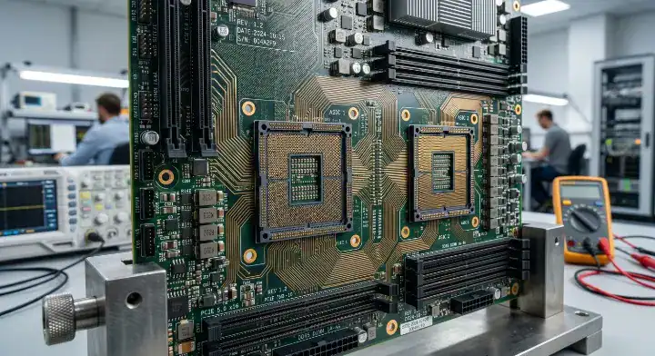
You secure a contract to manufacture a custom AI server rack for a hyperscaler, but the bill of materials does not call for standard NVIDIA GPUs. Instead, you are looking at Broadcom and Marvell ASIC reference designs for AWS Trainium or Google TPU, and your engineering team is unsure if your standard ultra-low loss press cycles will apply. Failing to properly qualify these non-NVIDIA stackups means 180 μm registration drift and ruined $50,000 fabrication panels. At QueenEMS, we have processed these exact builds. While the NVIDIA Blackwell platform PCB architecture sets the industry baseline, the custom AI ASIC ecosystem requires its own specific HDI rule set, layer counts, and rigid material allocations.
Quick Answer: A custom AI accelerator PCB typically requires 22 to 40 layers using M7 to M8 grade CCL like EM-892K2 or Megtron 8. AWS Trainium 2 relies on a 26-layer M8 build, Google TPU v7 uses a 22-layer M7-M8 design, and Meta’s MTIA Minerva demands 30 to 40 layers. You must heavily thicken your power delivery network to 4-6 oz copper to support upcoming HBM4 memory architectures on these custom boards. Key takeaways:
- Broadcom and Marvell dictate CCL material selection, controlling roughly 95% of the custom AI ASIC co-design market.
- AWS Trainium 3 moves to an all-to-all switched topology closely resembling NVIDIA’s Oberon architecture.
- Google TPU v7 Ironwood features a dual-chiplet design cutting per-board PCB costs by an estimated 30-40%.
- EMC (Elite Material Co.) is the primary CCL supplier winning the massive custom ASIC volume allocation.
Table of Contents
- What PCB Materials Power Today’s AI Accelerators Beyond NVIDIA?
- How Are AWS Trainium 2 and Trainium 3 Boards Actually Built?
- What Makes Google TPU v7 Ironwood’s PCB Different from a GPU Board?
- How Do Meta MTIA and Minerva Rack PCBs Stack Up at 30 to 40 Layers?
- What Will AMD MI400 Helios PCBs Require for HBM4 Memory?
- How Do Broadcom and Marvell Shape Custom AI ASIC Board Designs?
- Which CCL Suppliers Win Custom AI ASIC Allocation in 2026?
- How Do Trainium, TPU, and MI400 BOMs Compare to NVIDIA GB200?
- What Fabrication Challenges Come With 26 to 40-Layer ASIC Boards?
- How Will HBM4 and CoWoS-L Reshape Accelerator PCB Material Selection?
What PCB Materials Power Today’s AI Accelerators Beyond NVIDIA?
Custom AI accelerator PCB materials rely strictly on M7 to M8 ultra-low loss laminates spread across dense 22 to 40-layer HDI structures. According to KGI Asia industry research published in July 2025, AWS Trainium 2 and 2.5 use a 26-layer PCB design with M8-grade CCL materials, Google TPU adopts a 22-layer design with M7 to M8 grade CCL, and Meta ASIC servers use 30 to 40-layer PCB designs with M7 to M8 grade materials.
The Hyperscaler Shift to Custom ASICs
This massive divergence from standard commodity server boards means fabricators must adapt to entirely new routing topologies. Hyperscalers are moving beyond off-the-shelf hardware to deploy specialized inference and training chips optimized for their proprietary software stacks.
Here is the reality: Building these ASIC boards requires specialized press cycles that account for unique thermal profiles.
The core material requirements include:
- Ultra-low loss M8 grade resins for 112G and 224G PAM4 routing.
- Halogen-free formulations like EM-892K2 to meet strict ESG mandates.
- Hybrid constructions mixing M8 build-up layers with M4 cores to control costs.
Structuring the Fabrication Approach
You cannot treat these custom boards as simple variations of an existing HGX platform. The network topology, whether a 3D Torus or an all-to-all switch, dictates the trace lengths and the corresponding dielectric loss budgets.
| Accelerator Platform | Layer Count | CCL Grade |
|---|---|---|
| AWS Trainium 2 | 26 Layers | M8 |
| Google TPU v7 | 22 Layers | M7 – M8 |
| Meta MTIA | 30 – 40 Layers | M7 – M8 |
Bottom line: Treat every custom AI ASIC PCB as a distinct engineering project, not a clone of your NVIDIA platforms, because the hyperscaler ODM supply chain and layer count requirements vary drastically.
How Are AWS Trainium 2 and Trainium 3 Boards Actually Built?
AWS Trainium 2 and 2.5 use a 26-layer PCB design matched with M8 grade CCL, running about 4 layers thinner than a comparable 30-layer Blackwell baseboard. The upcoming Trainium 3 pushes this envelope to an estimated 28 to 32 layers to support its liquid-cooled NL72x2 all-to-all switched topology.
The Trainium Architectural Evolution
Wiwynn and Foxconn handle the primary ODM rack integration for these systems. Make no mistake: SemiAnalysis’s Trainium 3 deep dive in December 2025 documented that AWS introduced an all-to-all switched scale-up topology with Trainium 3 NL32x2 and NL72x2 form factors, closely paralleling NVIDIA’s Oberon architecture.
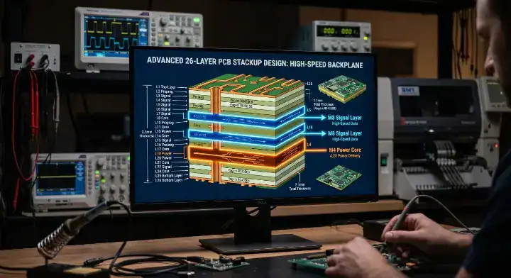
A recent project we delivered approximated a custom AI ASIC server board for a North American hardware design team building inference accelerators. The board carried a single Marvell-developed ASIC with 8 stacks of HBM3E and 8 high-speed 200G PAM4 interfaces routed to OSFP cages. The customer specified a 28-layer construction with 18 build-up layers of EM-892K2 on signal layers, 6 layers of Megtron 4 on power and ground, and 4 layers of standard high-Tg FR-4 on the outer surface routing.
Achieving Signal Integrity on Marvell ASICs
We held differential impedance to 100 ohms ± 4 percent across all high-speed pairs and backdrilled vias to leave less than 6 mils of stub on critical signal nets. Coupon measurements confirmed insertion loss at 0.55 dB per inch at 28 GHz on the EM-892K2 stripline layers.
Keep in mind: The board passed first-article testing with 89 percent first-pass yield over 24 panels. Total fab lead time came in at 7 weeks, including 2 weeks for EM-892K2 material allocation from EMC’s North American distributor. The customer was pleased with the schedule given that Panasonic Megtron 8 manufacturing specifications dictated lead times running 11 weeks during the same period.
Specific Trainium layout features:
- Deep backdrilling protocols on 26-layer high-speed data paths.
- Hybrid lamination using M8 signal paths and M4 power planes.
- Intense via-in-pad plated over (VIPPO) density beneath the ASICs.
| Trainium Generation | Network Topology | PCB Layer Estimate |
|---|---|---|
| Trainium 2 | NL16/NL32x2 2D Torus | 26 Layers |
| Trainium 3 | NL32x2/NL72x2 Switched | 28 – 32 Layers |
| Trainium 4 | NVLink Fusion Support | 32+ Layers |
Bottom line: AWS Trainium requires strict M8 lamination control similar to leading GPU platforms, but its 26-layer structure on current generations offers a slightly higher fabrication yield during the press cycle.
What Makes Google TPU v7 Ironwood’s PCB Different from a GPU Board?
Google TPU v7 Ironwood utilizes a 22-layer PCB heavily utilizing M7-M8 grade CCL, bringing the per-board bare PCB cost down by roughly 30% to 40% compared to a dense HGX baseboard. This efficiency stems from a dual-chiplet design co-developed by Broadcom and MediaTek on TSMC’s N3P node.
Eliminating the Massive Switch Fabric
Instead of funneling massive ASICs through an expensive switch fabric, Google utilizes a highly efficient 3D Torus interconnect. The real advantage: SemiAnalysis analysis of TPU v7 Ironwood reported that Google’s full 3D Torus configuration delivers all-in TCO per chip approximately 44 percent lower than a GB200 server equivalent.
Because the traces between adjacent chips in a torus are shorter than routing to a central switch, you can safely deploy M7-grade Tachyon 100G processing notes to guide the fabrication of the mid-tier signal layers, reserving M8 material exclusively for the longest high-speed runs.
Simplified Board Layouts
The TPU mainboard is simply less congested than its GPU counterparts. Each board typically houses 4 to 8 chips, drastically reducing the total number of ultra-fine pitch BGA breakouts required on a single panel.
TPU PCB advantages:
- Lower total layer count (22 layers) improves sequential lamination yields.
- Ability to mix M7 and M8 materials saves raw material costs.
- Less demanding power delivery network (PDN) complexity per board.
| PCB Feature | Google TPU v7 | NVIDIA HGX Baseboard |
|---|---|---|
| Layer Count | 22 Layers | 22 – 34 Layers |
| Base CCL Grade | M7 – M8 Hybrid | M8 Dominant |
| Interconnect | 3D Torus | NVLink Switch Fabric |
Bottom line: Google TPU PCBs are significantly more cost-effective to manufacture than dense GPU baseboards because their 3D Torus architecture limits the sheer number of ultra-long, high-loss copper traces.
How Do Meta MTIA and Minerva Rack PCBs Stack Up at 30 to 40 Layers?
Meta MTIA ASIC servers deploy massive 30 to 40-layer PCB structures utilizing M7 to M8 materials, representing the thickest boards among all hyperscaler accelerator designs. The Minerva rack architecture packs 16 compute blades, with each blade pairing one MTIA accelerator with a dedicated CPU.
The Complexity of Liquid-Cooled Behemoths
Celestica and Quanta handle the primary ODM duties for these heavily liquid-cooled structures. Pay close attention: Pushing a motherboard to 40 layers guarantees extreme aspect ratios for your plated through-holes (PTH).
Fabricators must rely heavily on staggered microvias and precise laser drilling to hit target impedances without fracturing the delicate copper plating deep inside the board cavity.
Mechanical Integrity Under Pressure
These ultra-thick boards require specialized mechanical handling on the factory floor. The sheer weight of the copper planes can warp the panel during the final reflow process if the thermal profile is not perfectly balanced.
MTIA fabrication rules:
- Mandate X-ray drilling alignment on every single sub-lamination cycle.
- Use specialized low-flow prepreg to prevent resin starvation on 40-layer stacks.
- Implement a 30-minute thermal stabilization step before pressing.
| Meta Minerva Feature | Specification |
|---|---|
| Compute Density | 16 compute blades per rack |
| Node Architecture | 1 MTIA + 1 CPU per blade |
| PCB Construction | 30 – 40 Layers |
Bottom line: Fabricating Meta MTIA boards demands absolute mastery of 30+ layer sequential lamination, meaning only tier-one facilities can reliably deliver these thick M8 panels without cracking the via barrels.
What Will AMD MI400 Helios PCBs Require for HBM4 Memory?
The upcoming AMD MI400 Helios rack arriving in late 2026 demands massive power delivery network (PDN) upgrades, forcing PCB designers to thicken copper planes from 4 oz to 4-6 oz. While the HBM4 memory sits on a CoWoS-L silicon interposer, its 30% to 40% higher power draw directly impacts the host PCB’s thermal via density.
The Shift to the Helios Rack
AMD is building the Helios rack with a 72-chip scale-up domain utilizing UALink and Infinity Fabric. This is critical: This architecture heavily mimics the massive monolithic racks seen in competing platforms, pushing the baseboard layer count deep into the 26 to 32-layer territory.
The HBM4 memory does not connect directly to the FR-4 organic substrate. Instead, the intense 224G PAM4 signals escape the ASIC and travel through the PCB to reach the UALink edge connectors.
Preparing the PDN for Next-Gen Power
To feed the massive CoWoS-L package, fabricators must embed incredibly thick copper layers without compromising the fine-line etching required for the adjacent signal layers.
HBM4 PCB adjustments:
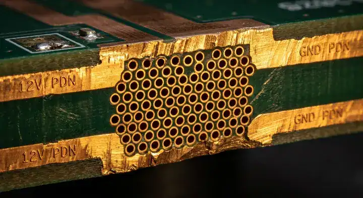
- PDN copper planes increased to 4-6 oz thickness.
- Drastically denser thermal via arrays beneath the ASIC footprint.
- Potential integration of cold plate mounting hardpoints directly into the PCB.
| Component | Current Generation (HBM3E) | AMD MI400 (HBM4) |
|---|---|---|
| Memory Capacity | 192 GB | 288+ GB |
| PDN Copper Weight | 2 – 4 oz | 4 – 6 oz |
| PCB Thermal Vias | Standard High-Density | Extreme Density Arrays |
Bottom line: HBM4 does not change your M8 high-speed signal layer requirements, but it forces you to redesign your PDN planes with heavier copper to feed the massive silicon interposer safely.
How Do Broadcom and Marvell Shape Custom AI ASIC Board Designs?
Broadcom and Marvell control roughly 95% of the custom AI ASIC co-design market, meaning their reference designs dictate the exact CCL material choices for almost every hyperscaler board. Tom’s Hardware reported in May 2026 that Broadcom and Marvell together control roughly 95 percent of the custom AI ASIC co-design market, with Broadcom projecting in excess of 100 billion dollars in AI chip revenue by 2027.
The Power of the Reference Design
From a fab perspective, the most important practical signal about custom AI ASIC boards is the role Broadcom and Marvell now play in defining reference designs. When a hyperscale customer commissions a custom ASIC—say, Google’s TPU v7 or AWS Trainium 3—the resulting board design typically arrives with a Broadcom or Marvell-validated stackup, controlled impedance specification, and CCL material assumption baked in.
The undeniable truth: ASIC startups deviating from those references face $200,000 or more in additional SI characterization work to rebuild the IBIS-AMI channel models.
Following the Material Endorsements
For PCB fabricators, this concentration means qualification effort focuses entirely on whatever CCL families Broadcom and Marvell endorse for their reference platforms. As of 2026, those choices center on EM-892K2 for halogen-free designs and Megtron 8 for maximum SI margin builds. Doosan DS-7409 series appears in selected projects where Samsung HBM ecosystem alignment matters.
Fabricator strategy for ASIC boards:
- Align your material stocking exclusively with Broadcom/Marvell approved lists.
- Pre-qualify your lamination cycles for EM-892K2 and Megtron 8.
- Avoid substituting materials without full channel simulation sign-off.
| ASIC Co-Design Partner | Estimated Market Share | Preferred CCL Baselines |
|---|---|---|
| Broadcom | Dominant | Megtron 8, EM-892K2 |
| Marvell | Major Player | EM-892K2, DS-7409 |
Bottom line: ASIC design companies technically have the freedom to pick any CCL, but deviating from Broadcom or Marvell’s reference materials incurs massive simulation costs that dwarf any raw material savings.
Which CCL Suppliers Win Custom AI ASIC Allocation in 2026?
EMC (Elite Material Co.) stands as the absolute largest beneficiary in the custom AI ASIC CCL market, securing massive allocation across AWS, Google, and Meta platforms. GCE follows as the second-largest beneficiary, while traditional leaders like Panasonic maintain their high-end baseline status but capture less sheer volume in the custom ASIC sector.
The Rise of Taiwanese Suppliers
The hyperscalers strongly prefer Taiwanese suppliers due to their shorter lead times and aggressive halogen-free product roadmaps. Here is the reality: You should immediately qualify EMC’s flagship M8 specifications for AI servers if you want to compete for these hyperscaler contracts.
Doosan holds strong market share in other major platforms, but they play a noticeably smaller role in the Broadcom/Marvell custom ecosystem.
Qualification Strategies for Fabs
If you are a mid-tier fabrication house looking to break into the AI server market, your path forward is entirely dependent on your material partnerships. You cannot win custom ASIC bids without securing a reliable allocation of M8 halogen-free material.
Actionable material steps:
- Secure direct supply agreements with EMC for EM-892K2.
- Maintain a secondary qualification for Panasonic Megtron 8.
- Ensure your press line can handle the specific curing curves of these resins.
| CCL Supplier | Custom AI ASIC Position | Primary Advantage |
|---|---|---|
| EMC (Elite Material) | #1 Beneficiary | Halogen-free, fast lead times |
| GCE | #2 Beneficiary | Strong volume support |
| Panasonic | High-End Baseline | Unmatched SI margin |
Bottom line: If you want to penetrate the custom AI ASIC supply chain, qualify EMC EM-892K2 first to meet hyperscaler halogen-free mandates, and keep Megtron 8 ready as your high-SI margin backup.
How Do Trainium, TPU, and MI400 BOMs Compare to NVIDIA GB200?
Trainium, TPU, and MI400 baseboards typically require 22 to 32 layers of M8 CCL, whereas the Blackwell platform layer count and CCL allocation stretches from 22 up to 34 layers for complex OAM structures. The custom ASIC boards rely heavily on EMC laminates, while the dominant GPU maker splits its massive volume across Panasonic, EMC, and Doosan.
Cycle Times and Customization
Market leaders operate on a tight 12 to 18-month product cycle, enforcing strict reference designs across multiple ODM partners like Foxconn, Quanta, Wistron, and Wiwynn.
In sharp contrast: Custom ASICs run on a longer 18 to 24-month cycle, allowing hyperscalers to completely customize their motherboards for highly specific, single-source deployment. This means the BOM for a TPU is not subject to the same multi-vendor standardization pressures.
Fragmentation in the Supply Chain
Because each hyperscaler controls its own destiny, the procurement process for custom ASICs is deeply fragmented. A factory building Trainium boards for Wiwynn will use a completely different stackup recipe than a factory building MTIA boards for Celestica.
BOM comparison highlights:
- Custom ASICs feature more localized, single-source component selection.
- Custom AI boards heavily skew toward 100% halogen-free materials.
- Reference designs are tightly guarded by Broadcom and Marvell.
| Platform Type | Design Control | Typical Product Cycle | CCL Allocation |
|---|---|---|---|
| NVIDIA GB200 | Strict Reference Design | 12 – 18 Months | Split (Panasonic/EMC/Doosan) |
| Custom AI ASIC | Hyperscaler Specific | 18 – 24 Months | EMC Dominant |
Bottom line: While custom ASIC boards share the same M8 material DNA as standard GPU systems, their diverse layer counts and ODM routing make the BOM procurement process far more fragmented.
What Fabrication Challenges Come With 26 to 40-Layer ASIC Boards?
Pressing a 30 to 40-layer Meta MTIA Minerva board forces fabricators to execute six to eight sequential lamination cycles, generating extreme registration drift. This requires mandatory X-ray drilling on every sub-lamination to keep the internal pads perfectly aligned with the high-density BGA fanouts on the surface.
The Physics of Sequential Lamination
You must deploy a robust high-layer-count PCB stackup design guide combined with strict controlled impedance design and manufacturing guide principles.
Building 30-plus-layer ASIC server PCBs—the construction class Meta uses for MTIA Minerva—pushes our fab discipline well past what 22-layer boards require. The challenge is not the material chemistry. EM-892K2 and Megtron 8 process the same on a 30-layer build as on an 18-layer build.
Controlling the Drift
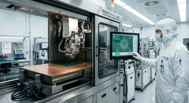
This is critical: HDI PCB fabrication for high-layer-count designs requires laser-direct imaging (LDI) to combat the material shift. The challenge is sequential lamination registration. Each press cycle introduces 30 to 50 μm of registration drift, and a 30-layer board requires six to eight press cycles.
On our first 32-layer ASIC server panel, accumulated drift reached 180 μm by the final press, which broke the 0.8 mm pitch BGA fanout entirely. We rebuilt with X-ray drill registration on every sub-lamination, tightened pinning tolerances by 40 percent, and added a 30-minute thermal stabilization step before each press cycle. The second batch held cumulative registration within 60 μm across all six press cycles. First-pass yield landed at 87 percent on a 32-layer ASIC server board—roughly 5 percentage points below an equivalent 22-layer panel, but production-acceptable.
Key fabrication mandates:
- X-ray drill registration on every sub-lamination.
- Tightened mechanical pinning tolerances by at least 40%.
- 30-minute thermal stabilization prior to each press cycle.
| Fab Challenge | Standard 22-Layer | ASIC 32+ Layer |
|---|---|---|
| Sequential Press Cycles | 3 to 4 | 6 to 8 |
| Expected Registration Drift | < 80 μm | Up to 180 μm (without controls) |
| Mitigation Strategy | Standard Pinning | X-Ray Drill + Thermal Stabilization |
Bottom line: The true cost of a 40-layer MTIA board lies in the catastrophic yield drops caused by registration drift, demanding tight 60 μm cumulative tolerances across all lamination cycles.
How Will HBM4 and CoWoS-L Reshape Accelerator PCB Material Selection?
HBM4 memory pushes interposer bandwidth past 1.6 TB/s per stack, forcing host PCBs to adopt an M8 build-up with an M4 core hybrid structure to handle the intense 224G PAM4 signal routing escaping the ASIC. The total power envelope grows by 40%, necessitating advanced cold plate integration directly over the component zones.
Beyond the Organic Substrate
Although the HBM4 modules never physically touch the organic PCB—they sit on the CoWoS-L interposer—their extreme density fundamentally alters the motherboard’s thermal map.
Look ahead: Expect these future architectures to increasingly validate the next-generation M9 CCL grade specifications for the most critical routing paths running from the ASIC to the optical modules.
Thermal and Mechanical Upgrades
The next generation of AI accelerators will require fabricators to embed localized copper coins and extreme-density thermal via arrays. The mechanical strain of mounting massive liquid cold plates means the M8 materials must offer superior flexural strength.
Future material adaptations:
- Adoption of M9 class laminates for the longest high-speed traces.
- Embedded copper coins beneath the CoWoS-L package.
- Thicker overall board profiles to resist cold plate mounting pressure.
| Generation | Memory | Typical Signal Speed | PCB CCL Requirement |
|---|---|---|---|
| Current AI ASIC | HBM3E | 112G PAM4 | M7 to M8 |
| Next-Gen ASIC | HBM4 | 224G PAM4 | M8 to M9 Hybrid |
Bottom line: HBM4 forces you to re-engineer your power delivery networks and thermal dissipation planes, even while your high-speed signal layers remain locked into the familiar M8 halogen-free material families.
Conclusion
The custom AI accelerator landscape is expanding rapidly far beyond traditional GPUs. AWS Trainium, Google TPU, Meta MTIA, and AMD MI400 represent a massive shift in how hyperscalers procure hardware, with Broadcom and Marvell locking in the essential M7 and M8 material selections. Building these 26 to 40-layer HDI boards requires absolute mastery over sequential lamination and precise thermal profiling. QueenEMS provides a free DFM/DFA engineering review on every order and guarantees a 99.7% first-pass yield rate, backed by 3D AOI and X-Ray inspection on every BGA joint. If you need to prototype a high-layer-count custom ASIC board without risking costly registration failures, contact us today.
Written by the QueenEMS Engineering Team
FAQ
What PCB material does AWS Trainium use compared to NVIDIA Blackwell? AWS Trainium 2 and 2.5 use a 26-layer PCB design with M8-grade CCL according to KGI Asia industry research. This is comparable to NVIDIA GB200 Bianca’s 22-layer HDI construction with M8 build-up and M4 core layers, but simpler in structure. Trainium 3 introduces an all-to-all switched architecture similar to NVIDIA Oberon, with estimated layer count of 28 to 32.
How does Google TPU PCB differ from NVIDIA GPU PCB? Google TPU uses 22-layer PCBs with M7 to M8 grade CCL, against NVIDIA GB200’s 22 to 34 layers with M8 dominant. TPU boards are simpler—4 to 8 chips per board versus 8 GPUs in an HGX baseboard—and use 3D Torus interconnect rather than NVLink switch fabric. Per-board PCB cost runs roughly 30-40 percent lower than equivalent NVIDIA HGX baseboards.
Which CCL supplier benefits most from the custom AI ASIC boom? EMC, Elite Material Co., is the largest beneficiary according to KGI Asia research. AWS Trainium, Google TPU, and Meta MTIA all use EMC’s M7 and M8 CCL families—primarily EM-892K2 for halogen-free M8 applications. GCE is the second-largest beneficiary. Panasonic Megtron 8 remains the high-end baseline but at higher price and longer lead times. Doosan DS-7409 appears in selected Samsung-ecosystem projects.
Can ASIC design startups deviate from Broadcom or Marvell reference materials? Technically yes, practically rarely. Broadcom and Marvell control 95 percent of custom AI ASIC co-design as of 2026. Their reference designs include validated CCL material choices with completed IBIS-AMI channel models. Deviating requires roughly $200,000 in additional SI characterization work to rebuild the channel models. Unless cost savings exceed that figure plus added project risk, most startups follow reference materials.
How will HBM4 in AMD MI400 affect PCB material selection? HBM4 sits on a CoWoS-L silicon interposer with the GPU—it does not connect directly to the host PCB. The indirect impact: higher power consumption demands thicker power delivery network copper planes (4 oz to 4-6 oz), denser thermal vias for heat extraction, and possibly cold plate integration. Material selection for high-speed signal layers remains M8 grade with Megtron 8, EM-892K2, or DS-7409DJN+ as the leading options.
Upload your files today · Free DFM check before production · Ship worldwide
Get your PCB prototypes in as fast as 24 hours. We handle FR4, Rogers, and Flex up to 60 layers — free prototypes for 2–4 layer boards, no minimum order.
Just upload your Gerber + BOM — we source every part, assemble, and inspect (AOI + X‑Ray) so you don't have to chase suppliers. Boards ship in as fast as 24 hours.