
Many hardware engineering teams designing infrastructure around the latest AI platforms struggle to define the exact bare-board specifications required to survive 120 kW rack densities. Without accurate data on layer counts, laminate grades, and structural architecture, system integrators often over-engineer their peripheral boards or severely underestimate their manufacturing budgets. Understanding the precise NVIDIA Blackwell PCB material breakdown provides the only realistic baseline for launching compatible 800G and 1.6T hardware.
Table of Contents
- #1 What PCB Materials Does the NVIDIA Blackwell Platform Use?
- #2 How Is the GB200 Bianca Board Built and What Layers Use M8?
- #3 How Does the GB300 UBB and OAM Differ from the GB200 Design?
- #4 What Makes M8-Grade CCL the Default for Blackwell Compute Boards?
- #5 Where Do Megtron 8, EM-892K2, and DS-7409 Fit in Blackwell BOMs?
- #6 How Are NVSwitch Trays and 1.6T Line Cards Built?
- #7 What Stackup and Layer-Count Decisions Drive Blackwell PCB Costs?
- #8 What Design Rules Apply to 200 Gbps NVLink 5.0 Channels?
- #9 Where Does the Supply Chain Stand for Blackwell PCB Manufacturing?
- #10 How Will Rubin and Rubin Ultra Change Blackwell-Era Material Choices?
What PCB Materials Does the NVIDIA Blackwell Platform Use?
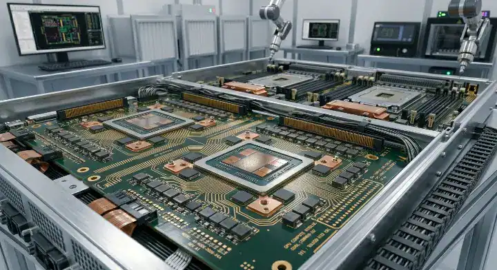
The Blackwell ecosystem relies on a rigid combination of M8-grade and M4-grade laminates to manage the massive bandwidth required by the B100, B200, and GB200 architectures. SemiAnalysis’s GB200 hardware architecture documentation details that the NVL72 rack integrates 18 compute trays and 9 NVSwitch trays, demanding extreme signal integrity across every interconnect. This hardware generates 120 kW of power per single cabinet, forcing all PCB materials to prioritize extreme thermal stability over raw cost savings.
The M-Series Mapping
The platform strictly categorizes its board layers into distinct performance tiers, mapping specifically to the M-series specification. Instead of applying ultra-low-loss materials blindly across every copper layer, engineers apply hybrid stackups. Consider the platform standards:
- M8-grade laminates surround the critical NVLink 5.0 and PCIe Gen6 channels.
- M4-grade laminates handle power delivery and ground planes.
- This hybrid strategy prevents the bill of materials from escalating out of control. Key Takeaway: Understanding which data lanes physically require the premium M8 chemistry protects your procurement budget from unnecessary spending on slow-speed control layers.
NVL72 Rack Component Breakdown
Deploying an NVL72 system requires multiple distinct PCB architectures, each with its own material challenges. The compute tray houses the primary processors, while the NVSwitch tray acts as the spine of the network, routing 28.8 Tb/s of data per ASIC. Key Takeaway: Designing compatible hardware requires studying the specific material constraints of the board you intend to interface with, as a compute board stackup differs wildly from a switch board.
| System Component | PCB Function | Primary Material Grade |
|---|---|---|
| Compute Tray | Houses GPUs & Grace CPU | M8 Build-up + M4 Core |
| NVSwitch Tray | Routes NVLink Traffic | M8 Signal + M4 Core |
| OSFP Host Board | Manages 800G/1.6T Optics | M7 to M8 Grade |
| Analysis: The entire physical network relies on the M8 specification to guarantee zero-defect data transmission across the rack. |
Bottom line: The Blackwell platform standardizes strictly on hybrid M8 and M4 constructions to balance 200 Gbps signal integrity against severe thermal loads.
How Is the GB200 Bianca Board Built and What Layers Use M8?
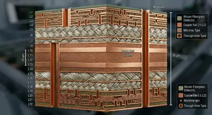
What is the actual layer count and material breakdown of a GB200 Bianca board? A Bianca board is the 22-layer HDI compute board that anchors GB200 trays, built with 18 layers of M8-grade laminate and 4 layers of M4-grade core, supplied primarily by Unimicron and Victory Giant. This specific HDI PCB manufacturing capability requires aggressive sequential lamination to route the massive pin count of the superchip.
The 22-Layer HDI Structure
The Bianca design forces fabricators to execute multiple pressing cycles to build up the microvia structures required to escape the GPU footprint. The design permanently solders the Blackwell GPUs and Grace CPU directly to the substrate, maximizing electrical performance but creating significant repairability challenges for the ODM. Analyze the build structure:
- The board utilizes 18 layers of M8-grade material specifically for high-speed routing.
- The central core relies on 4 layers of M4-grade material to manage power and rigidity.
- The estimated bare-board ASP exceeds $1000 due to the extreme sequential lamination yield loss. Key Takeaway: Attempting to replicate this design requires a fabrication partner fully qualified in executing 20+ layer HDI builds with extreme registration tolerances.
Yield and Manufacturing Risks
Soldering highly expensive silicon directly to a massive 22-layer board means a single bare-board defect destroys thousands of dollars in components. Fabricators face immense pressure to deliver 100% electrically tested panels with zero microvia latent defects. Key Takeaway: If you are designing peripheral hardware that interfaces with Bianca, your design rules must account for the extreme routing density of the host system.
| Bianca Characteristic | Value / Spec | Factory Impact |
|---|---|---|
| Layer Count | 22-Layer HDI | High sequential press cycles |
| Material Ratio | 18x M8 : 4x M4 | Complex hybrid lamination |
| GPU Mounting | Direct SMT | Near-zero reworkability |
| Primary Suppliers | Unimicron, Victory Giant | Severe allocation limits |
| Analysis: The Bianca design trades manufacturing simplicity for absolute maximum electrical performance within the compute tray. |
Bottom line: The GB200 Bianca relies on an uncompromising 22-layer HDI structure dominated by M8 materials, presenting a massive manufacturing barrier for standard fab shops.
How Does the GB300 UBB and OAM Differ from the GB200 Design?
Why did NVIDIA shift from the monolithic Bianca board to a modular structure for the next hardware iteration? The GB300 UBB (Universal Base Board) returns to a modular design, featuring an 18-layer PTH construction utilizing 14 layers of M8 and 4 layers of M4, holding an ASP of roughly $750-800. This modularity allows ODMs to use sockets for the GPUs, drastically improving repairability and assembly yield on the factory floor.
The Modular GB300 Architecture
The GB300 separates the main processing units onto OAM (OCP Accelerator Module) cards that plug into the UBB. The high-end OAM module features a 20-layer PTH design, while the low-end variant uses a 16-layer HDI structure. Review the architectural shift:
- UBB: 18 layers, PTH technology, supplied heavily by WUS and TTM.
- High-End OAM: 20 layers, PTH, 16x M8 and 4x M4.
- Low-End OAM: 16 layers, HDI, 12x M8 and 4x M4. Key Takeaway: This hardware segmentation allows hardware designers to target their board capabilities specifically against the intended compute tier.
Platform Volatility
According to Tom’s Hardware reporting in May 2025, NVIDIA reverted the GB300 from the Cordelia chip board layout to the older Bianca design following installation issues reported by suppliers, demonstrating that Blackwell PCB architecture is still in flux. Signal transmission issues through the socket connectors constantly force engineering teams to re-evaluate the monolithic versus modular debate. Key Takeaway: System integrators must maintain flexible supply chains capable of pivoting between PTH baseboards and complex HDI structures depending on NVIDIA’s final reference design.
| GB300 Component | Layer Count & Tech | Material Ratio | Estimated ASP |
|---|---|---|---|
| UBB Baseboard | 18-Layer PTH | 14x M8 / 4x M4 | $750 – $800 |
| High-End OAM | 20-Layer PTH | 16x M8 / 4x M4 | High Premium |
| Low-End OAM | 16-Layer HDI | 12x M8 / 4x M4 | Mid Premium |
| Analysis: Modular designs shift the engineering burden from the bare-board HDI lamination process onto the physical connector SI validation. |
Bottom line: The GB300 transitions to a UBB/OAM structure to solve ODM repairability issues, though signal integrity challenges keep the final board specifications highly volatile.
What Makes M8-Grade CCL the Default for Blackwell Compute Boards?
Why does the hardware ecosystem refuse to utilize legacy Megtron 6 materials on these specific builds? Panasonic’s MEGTRON family covers the full M4-to-M8 grade range used across the Blackwell platform: MEGTRON 4 (R-5725) for core layers, MEGTRON 8 (R-5795) for high-speed build-up layers. The extreme bandwidth of the architecture physically destroys signals routed over anything with a dissipation factor higher than 0.0015.
The Physics of the M-Series
The M-series designation dictates strict limits on dielectric loss and phase skew. When routing 100 GB/s per lane, the bare board acts as an active physical constraint on data transmission. You can review the exact specifications in our dedicated Megtron 8 PCB manufacturing guide. Consider the material science:
- M6 delivers a Df around 0.002, completely failing 200 Gbps channel budgets.
- M8 pushes Df down to 0.0010-0.0012, utilizing modified PPO resins.
- M8 mandates NER-glass to prevent severe glass-weave skew on differential pairs. Key Takeaway: The transition to M8 is not a marketing upgrade; it is a rigid physics requirement to prevent signal collapse across the backplane.
The Transition to M8.5 and Beyond
As trace lengths increase, even standard M8 chemistry struggles to maintain an open data eye. The industry expects to transition toward the next-generation M9 CCL grade for the upcoming Rubin architectures to hit sub-0.0007 Df targets. Key Takeaway: Base your long-term procurement strategy on establishing relationships with fabricators who actively stock M8 materials today, as they will receive priority allocation for M9 tomorrow.
| Laminate Tier | Representative Product | Target Df | Platform Fit |
|---|---|---|---|
| M6 Grade | Megtron 6 | 0.0020 | Hopper / 400G |
| M7 Grade | Megtron 7 | 0.0015 | H200 / 800G |
| M8 Grade | Megtron 8 | 0.0012 | Blackwell / 1.6T |
| Analysis: The M8 grade sits at the absolute limit of what non-quartz glass structures can physically support. |
Bottom line: The M8 specification provides the exact combination of low-loss resin and uniform glass weave required to make the Blackwell platform electrically viable.
Where Do Megtron 8, EM-892K2, and DS-7409 Fit in Blackwell BOMs?
Can I use EM-892K2 or SH G7 or DS-7409 to substitute for Megtron 8 in a Blackwell-class board? Yes, DS-7409DJN+ from Doosan and EM-892K2 from Elite Material are already qualified at NVIDIA for selected Bianca and OAM layers, delivering Df values between 0.0013 and 0.0014. While the Panasonic R-5795 specifications serve as the gold standard, severe allocation limits force ODMs to rely heavily on these alternative M8-grade laminates.
Substituting Across the Stackup
Not every M8 layer performs the same critical function. The specific NVLink 5.0 SerDes channels demand absolute minimum insertion loss, often locking them exclusively to Panasonic’s chemistry. Evaluate substitution rules:
- Megtron 8 remains the default for the absolute longest, highest-speed NVLink runs.
- EM-892K2 dominates the 800G/1.6T switch line card market due to better availability.
- DS-7409DJN+ secured early qualification and powers massive portions of the GB200 build.
- SH G7 offers a massive cost advantage for less critical inference servers. Key Takeaway: You must run your channel simulation against the exact Dk and Df of the proposed substitute material, as slight variations will throw off your 100 Ω impedance targets.
The Role of M4 Cores
Beneath the high-speed outer layers, massive M4 cores act as the mechanical and power-delivery foundation. Megtron 4 is the legacy choice, but fabricators frequently substitute highly rigid FR-4 equivalents to manage costs without impacting signal integrity. Key Takeaway: Focus your premium material budget exclusively on the critical nets, aggressively substituting cheaper materials on power and ground layers to control your ASP.
| Supplier | Product Line | Df @ 10 GHz | Blackwell Application |
|---|---|---|---|
| Panasonic | Megtron 8 | 0.0010 – 0.0012 | Critical SerDes / NVLink |
| Doosan | DS-7409DJN+ | 0.0013 | Bianca board bulk |
| EMC | EM-892K2 | 0.0014 | Switch line cards |
| Shengyi | SH G7 | 0.0014 | Cost-sensitive inference |
| Analysis: The supply chain absolutely requires multiple qualified M8 suppliers to prevent a single chemical plant from stalling global AI deployments. |
Bottom line: While Megtron 8 holds the highest specification, EM-892K2 and DS-7409DJN+ serve as heavily relied-upon substitutes across the vast majority of the Blackwell ecosystem.
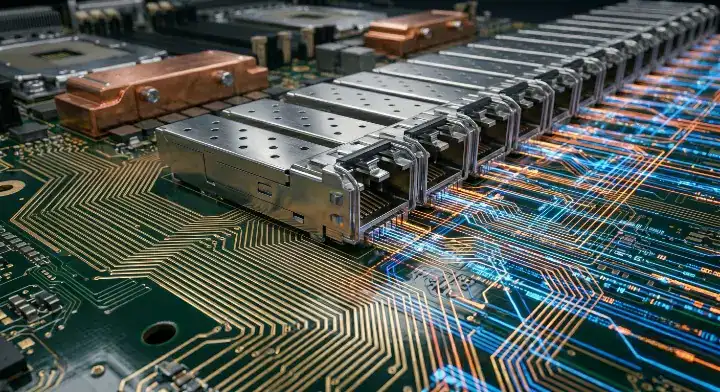
How Are NVSwitch Trays and 1.6T Line Cards Built?
What materials drive the massive interconnect spine sitting at the center of the NVL72 rack? The NVSwitch tray manages 18 individual 1.6T twin-port OSFP cages, demanding a multi-layer hybrid construction built primarily on M8-grade signal layers and M4-grade power cores. Per IEEE 802.3 800GBASE-R specifications, the host PCB channel insertion loss at 28 GHz Nyquist for 224G-PAM4 lanes establishes the practical floor for laminate Df at 0.0015 — placing M8-grade materials as the entry-level choice for NVSwitch tray host boards.
A 1.6T Line Card Case Study
A recent build we delivered was an 18-layer NVSwitch-class line card for a customer designing 1.6 Tbps switching infrastructure outside the NVIDIA reference design. The board used 12 layers of M8-grade laminate on the SerDes signal layers carrying 112 Gbps PAM4, plus 6 layers of M4-equivalent material for power and ground. Differential impedance was held at 100 Ω ± 4% across all NVLink-compatible pairs, and backdrill depth left under 6 mils of via stub on all critical signals. Here are the field results:
- The qualification coupon measured 0.54 dB/inch at 28 GHz on 4 mil stripline.
- Total fab lead time sat at 8 weeks due to M8 material allocation.
- We utilized similar processing controls as our Tachyon 100G material specifications builds to ensure ultra-smooth copper adhesion. Key Takeaway: Building compatible switch infrastructure requires mastering precise backdrilling to prevent via stubs from destroying the 200 Gbps signal reflection.
OSFP Host Board Material
The peripheral boards hosting the optical transceivers also demand extreme material performance to interface cleanly with the main NVSwitch ASICs. These boards typically float between M7 and M8 grades, depending strictly on the physical distance between the ASIC and the OSFP cage. Key Takeaway: Never design an OSFP host board on M6 materials if it intends to interface with a Blackwell-generation switch, as the insertion loss will break the link.
| Component Type | Primary Function | CCL Grade Required | Key Fabrication Control |
|---|---|---|---|
| NVSwitch Tray | ASIC routing | M8 / M4 Hybrid | Backdrill Depth |
| 1.6T Line Card | External switching | M8 | Copper Roughness |
| OSFP Host PCB | Optical interface | M7 / M8 | Impedance Tolerance |
| Analysis: The routing complexity of the switch architecture demands absolute perfection in via stub removal to prevent resonant signal failure. |
Bottom line: The NVSwitch architecture relies on thick, hybrid M8 stackups combined with surgical backdrilling to support the massive density of 1.6T OSFP interconnects.
What Stackup and Layer-Count Decisions Drive Blackwell PCB Costs?
Why do these specific AI motherboards cost vastly more than legacy server infrastructure? Running a 22-layer HDI build that approaches the complexity of a Bianca-class compute board exposes how thin the margin is in this part of the industry, as each sequential lamination cycle exponentially increases the risk of catastrophic scrap. Fabricating a single GB200-class board demands flawless registration across multiple pressing phases.
Registration and Yield Realities
Our team built a 22-layer test panel with 18 layers of M8-grade laminate and 4 layers of M4 core in the same construction NVIDIA uses for GB200 Bianca boards — same HVLP3 copper, same NER-glass spread weave, same sequential lamination cycle. First-pass yield landed at 88% on the initial run, limited by registration drift between the 8th and 10th lamination press cycles. Consider the process adjustments:
- We pulled yield up to 94% on the third batch by tightening X-ray drill registration.
- We added a 30-minute thermal soak before each press cycle to stabilize prepreg moisture.
- The Bianca-class boards require extreme discipline, not necessarily exotic press recipes. Key Takeaway: Demand detailed cross-section reports from your fabricator proving their inner-layer registration capabilities before awarding them a high-layer-count HDI contract.
The Cost of Hybrid Lamination
The requirement to mix highly rigid M4 cores with softer, resin-rich M8 outer layers creates immense mechanical stress during the cooling phase of lamination. If the fabricator fails to balance the copper density perfectly, the board will warp, completely ruining the subsequent BGA assembly process. Key Takeaway: Your PCB design team must perfectly balance the copper pours on your hybrid stackups to prevent the fabricator from scrapping the panels due to severe bowing.
| Stackup Variable | Legacy Server | Blackwell Class | Cost Impact |
|---|---|---|---|
| Layer Count | 12 to 16 | 18 to 22 | High |
| Material Grade | FR4 / M4 | M8 / M4 Hybrid | Extreme |
| Copper Foil | Standard RTF | HVLP3 / HVLP4 | High |
| Analysis: The convergence of high layer counts, premium chemistry, and ultra-smooth copper creates a multiplier effect on the final bare-board price. |
Bottom line: The astronomical cost of Blackwell PCBs stems directly from the severe yield drops associated with repeatedly pressing 22 layers of dissimilar laminates.
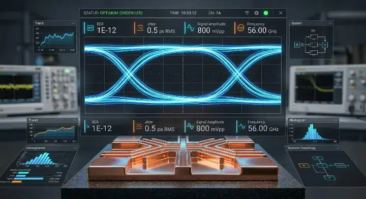
What Design Rules Apply to 200 Gbps NVLink 5.0 Channels?
What are the real PCB design rules for 200 Gbps NVLink 5.0 channels? Engineering an NVLink 5.0 channel requires locking differential impedance to 100 Ω ± 5%, driving intra-pair skew below 5 ps, and mandating via stub lengths strictly under 10 mils via backdrilling. These metrics are significantly tighter than legacy PCIe standards and completely define the mechanical constraints of your layout.
Strict Routing Parameters
The 200 Gbps PAM4 SerDes operating at 28 GHz Nyquist offers virtually zero margin for layout errors. Standard ED copper is absolutely unacceptable on these signal layers; you must specify HVLP3 or HVLP4 foils to eliminate the skin effect. Follow these rigid rules:
- Trace widths must sit between 75-100 µm (3-4 mil) on inner stripline layers.
- Differential pair spacing must be ≥ 2× the trace width to prevent crosstalk.
- Intra-pair skew must remain under 5 ps for NVLink 5.0 and under 3 ps for PCIe Gen6. Key Takeaway: If your layout tool lacks automated phase-matching and skew-checking capabilities, you will fail to route a functional NVLink channel.
The Backdrilling Mandate
Any copper via barrel extending past the active signal layer acts as an antenna, creating destructive resonance that collapses the data eye. Fabricators must utilize precision depth-controlled backdrilling to remove these stubs. Ideally, the remaining stub should measure under 5 mils on critical traces. Key Takeaway: Provide your fabricator with a highly detailed backdrill table calling out the specific start and stop layers for every single high-speed via.
| Design Parameter | NVLink 5.0 Requirement | Typical Factory Capability |
|---|---|---|
| Impedance | 100 Ω ± 5% | ± 10% (Requires tuning) |
| Via Stub | < 10 mils | ~8 mils (Depth controlled) |
| Copper Foil | HVLP3 / HVLP4 | RTF (Requires upgrade) |
| Analysis: The design rules demand absolute perfection in both the digital layout file and the physical chemical etching process. |
Bottom line: NVLink 5.0 channels require an uncompromising adherence to tight impedance tolerances, ultra-smooth copper, and aggressive stub removal to function.
Where Does the Supply Chain Stand for Blackwell PCB Manufacturing?
Can a Tier-2 or Tier-3 PCB fab actually win allocation for a Blackwell-class board? Direct allocation for Bianca and UBB boards is heavily concentrated at four Tier-1 fabs—Unimicron, WUS, TTM, and Victory Giant—leaving smaller shops locked out of the primary hardware runs. However, Tier-2 and Tier-3 fabs have highly realistic opportunities in secondary sourcing for NVSwitch line cards, optical module host PCBs, and power management boards.
The Tier-1 Monopoly
The sheer volume of capital required to build 22-layer sequential lamination boards reliably naturally filters out 95% of global fabricators. NVIDIA relies on a tight ecosystem of established players who already hold massive inventory allocations of Megtron 8 and EM-892K2. Understand the supplier mapping:
- Unimicron and Victory Giant dominate the Bianca board output.
- WUS and TTM control the vast majority of the GB300 UBB volume.
- These Tier-1 shops receive priority prepreg allocation directly from Panasonic and Doosan. Key Takeaway: Do not attempt to source your primary Bianca-clone prototypes from a generic fab shop; they will fail the material allocation stage before ever drilling a hole.
Finding Tier-2 Opportunities
If you are developing peripheral hardware or competing in the 1.6T switch market, highly capable mid-tier fabs offer better engineering support and faster prototype lead times. Entry into this space requires the fab to possess verified 22+ layer capability and active accounts with M8 distributors. Key Takeaway: Audit your prospective fab partner strictly on their HVLP3 copper handling and their documented history of processing M8-equivalent laminates at production scale.
| Fab Tier | Target Blackwell Component | Expected Lead Time | Material Access |
|---|---|---|---|
| Tier 1 | Bianca / GB300 UBB | OEM Dedicated | Direct Allocation |
| Tier 2 | NVSwitch / OSFP Hosts | 6 – 8 Weeks | Distributor Allocation |
| Tier 3 | Power / Management Boards | 3 – 5 Weeks | Open Market (M4) |
| Analysis: The hardware supply chain heavily segments its manufacturing based strictly on the fab’s access to highly restricted raw materials. |
Bottom line: While Tier-1 shops monopolize the core compute boards, mid-tier fabricators remain highly viable partners for the massive ecosystem of peripheral switch and optical hardware.
How Will Rubin and Rubin Ultra Change Blackwell-Era Material Choices?
What material replaces the M8 standard when hardware inevitably demands even faster signaling? The upcoming Rubin and Rubin Ultra platforms will force the industry to abandon standard glass weaves entirely, adopting the ultra-low-loss laminate for next-gen AI boards known as the M9 CCL specification. This transition introduces massive new fabrication challenges regarding quartz-glass drilling and prepreg adhesion.
The Shift to M9 and Q-Glass
The Rubin architecture plans to utilize massive orthogonal backplanes to handle the increased bandwidth, pushing trace lengths to absolute physical extremes. To hit the required sub-0.0007 Df, the M9 specification mandates the use of Q-glass (quartz fiber) and HVLP4/5 copper foils. Review the future challenges:
- Doosan’s DS-7409 M9Q variant currently leads the M9 qualification race.
- Quartz glass dramatically reduces drill bit lifespan, increasing fabrication costs.
- Allocation for M9 prepregs will be even tighter than current M8 supplies. Key Takeaway: Engineering teams must establish strong feedback loops with their current M8 fabricators to ensure those shops are actively testing M9 coupons today.
The Orthogonal Backplane Hurdle
The Rubin Ultra platform utilizes an incredibly thick, multi-board pressed orthogonal backplane designed to eliminate long internal trace routing. This structure requires pressing multiple fully assembled inner boards together, a process that carries severe thermal and mechanical risks. Key Takeaway: The era of simple, monolithic AI motherboards is ending, replaced by modular, extreme-layer-count structures that act more like physical chassis than traditional circuit boards.
| Platform | Expected Timeline | Primary CCL Spec | Key Structural Feature |
|---|---|---|---|
| GB200 / GB300 | Current | M8 Grade | 22-Layer HDI / UBB |
| Rubin (Standard) | 2026 | M8.5 / M9 Eval | Advanced Switch Trays |
| Rubin Ultra | 2026 H2 | M9 Grade | Orthogonal Backplane |
| Analysis: The relentless push for bandwidth forces laminate chemistry to evolve faster than standard factory machining equipment can adapt. |
Bottom line: The Rubin transition will aggressively phase out standard M8 materials on the most critical paths, forcing the entire supply chain to master quartz-blended M9 laminates.
Conclusion
Mastering the physical infrastructure of the AI revolution requires understanding exactly how the NVIDIA Blackwell platform utilizes materials to solve extreme signal and thermal constraints. By studying the precise M8/M4 hybrid constructions of the GB200 Bianca and GB300 UBB boards, hardware engineers can accurately specify their own compatible switch and peripheral layouts. We execute these extreme high-speed builds daily, bridging the gap between rigorous SI requirements and actual factory-floor yield. If your next project demands NVLink 5.0 performance or 22-layer HDI reliability without the standard prototype guesswork, contact us today to review your stackup design. QueenEMS remains dedicated to delivering transparent, data-driven fabrication solutions that protect your SI margins and secure your position in the AI hardware supply chain.
FAQ
What PCB material is used in the GB200 Bianca board? The GB200 Bianca board is a 22-layer HDI construction using 18 layers of M8-grade laminate (such as Megtron 8 R-5795) for the high-speed build-up layers and 4 layers of M4-grade material (such as Megtron 4 R-5725) for the core. Primary fabricators are Unimicron in Taiwan and Victory Giant Technology in mainland China.
How much does a GB300 UBB PCB cost? The GB300 UBB has an ASP of approximately $750-800 per board for an 18-layer PTH construction with 14 M8-grade layers and 4 M4-grade core layers. Primary suppliers are WUS in mainland China and TTM in the United States. Pricing reflects high-layer-count, M8 material premium, and tight controlled impedance tolerances.
Can I use EM-892K2 or DS-7409DJN+ instead of Megtron 8 in a Blackwell-class board? On most Blackwell BOM positions, yes. DS-7409DJN+ from Doosan and EM-892K2 from Elite Material are already qualified at NVIDIA for selected Bianca and OAM layers. They deliver Df at 0.0013-0.0014 versus Megtron 8’s 0.0010-0.0012. The NVLink 5.0 critical SerDes layers may still default to Megtron 8 for SI margin, but power, ground, and lower-speed layers accept substitutes.
What are the design rules for 200 Gbps NVLink 5.0 channels? Differential impedance 100 ohms plus or minus 5 percent, intra-pair skew under 5 picoseconds, via stub length under 10 mils after backdrilling (ideally under 5 mils on critical traces), HVLP3 or HVLP4 copper foil mandatory, trace width 75-100 micrometers on inner stripline layers. Standard ED copper is not acceptable on NVLink 5.0 signal layers.
Can a smaller PCB fab win allocation for Blackwell-class boards? Direct allocation for Bianca and UBB boards is concentrated at four Tier-1 fabs (Unimicron, WUS, TTM, Victory Giant). Tier-2 and Tier-3 fabs have realistic opportunities in NVSwitch line card secondary sourcing, 800G and 1.6T OSFP host PCBs, and ancillary power and management boards. Entry requires qualified 22-plus-layer HDI sequential lamination capability and at least one M8-grade construction qualification.
Upload your files today · Free DFM check before production · Ship worldwide
Get your PCB prototypes in as fast as 24 hours. We handle FR4, Rogers, and Flex up to 60 layers — free prototypes for 2–4 layer boards, no minimum order.
Just upload your Gerber + BOM — we source every part, assemble, and inspect (AOI + X‑Ray) so you don't have to chase suppliers. Boards ship in as fast as 24 hours.